Semiconductor device and display device

a semiconductor device and display device technology, applied in semiconductor devices, instruments, electrical apparatus, etc., can solve the problems of static electricity, deterioration in production yield caused by static electricity, and static electricity, so as to prevent electrostatic damage

Inactive Publication Date: 2014-01-30
SHARP KK
View PDF2 Cites 9 Cited by
  • Summary
  • Abstract
  • Description
  • Claims
  • Application Information

AI Technical Summary

Benefits of technology

[0022]According to the present invention, there is provided a semiconductor device having an oxide semiconductor TFT in which electrostatic damage is prevented, and a display device having such a semiconductor device.

Problems solved by technology

On the other hand, the fabrication process of a semiconductor device includes steps which are liable to static electricity.
Static electricity may induce changes in characteristics or electrostatic discharge failures, thus resulting in a problem in that the production yield of semiconductor devices having the TFTs may be deteriorated.
Deterioration in production yield caused by static electricity that occurs is particularly a problem in the TFT substrate (semiconductor device) of a liquid crystal display device.

Method used


Image

  • Semiconductor device and display device
  • Semiconductor device and display device
  • Semiconductor device and display device

Examples


Embodiment Construction

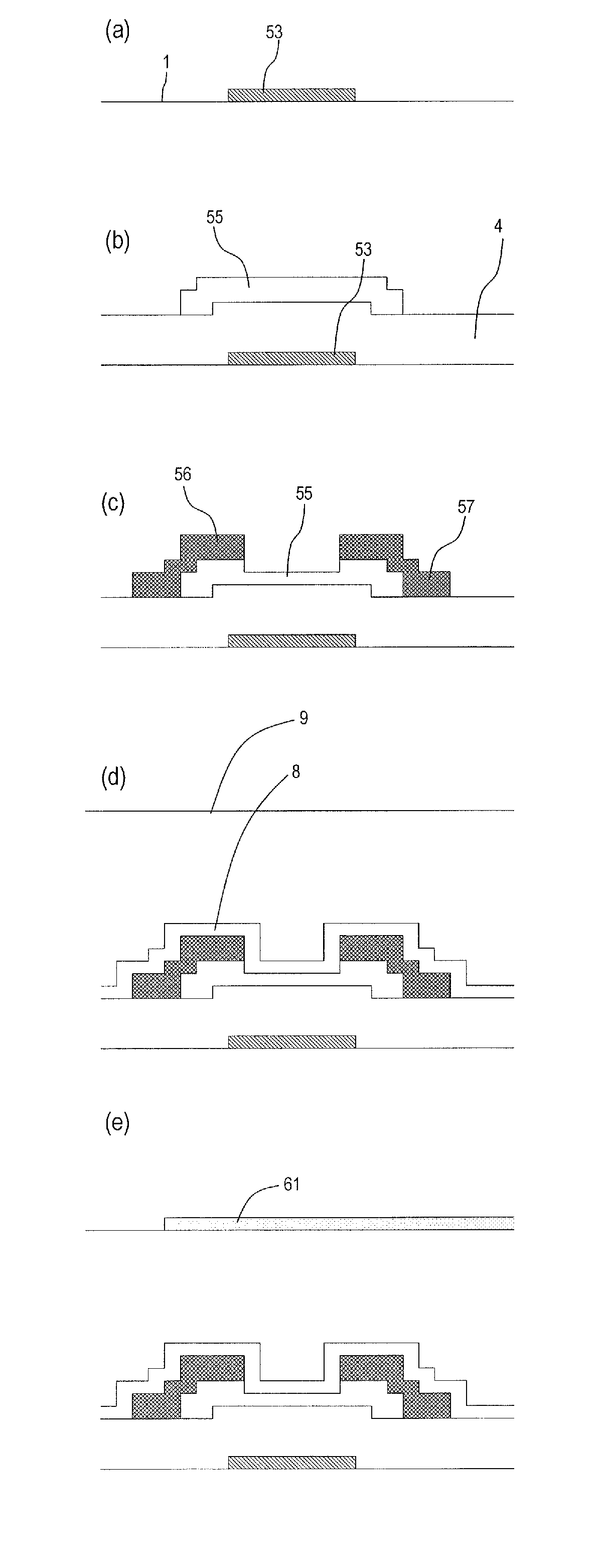
[0029]Hereinafter, with reference to the drawings, a production method for a semiconductor device according to an embodiment of the present invention and the construction of a semiconductor device which is produced by that production method (which herein is a TFT substrate for a liquid crystal display device) will be described. The TFT substrate in the present embodiment encompasses TFT substrates of various display devices (e.g., liquid crystal display devices and EL display devices).

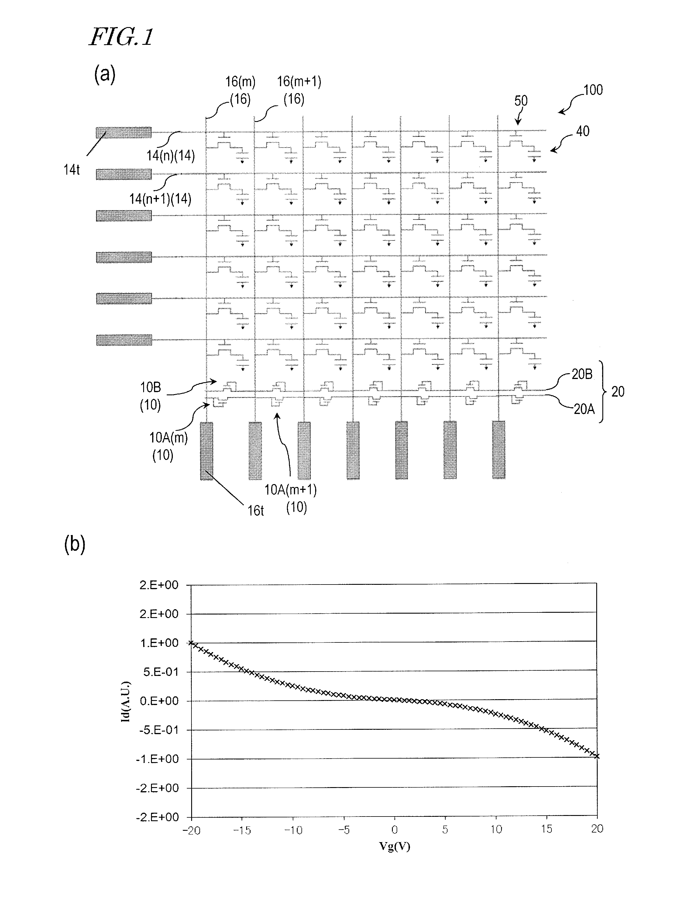
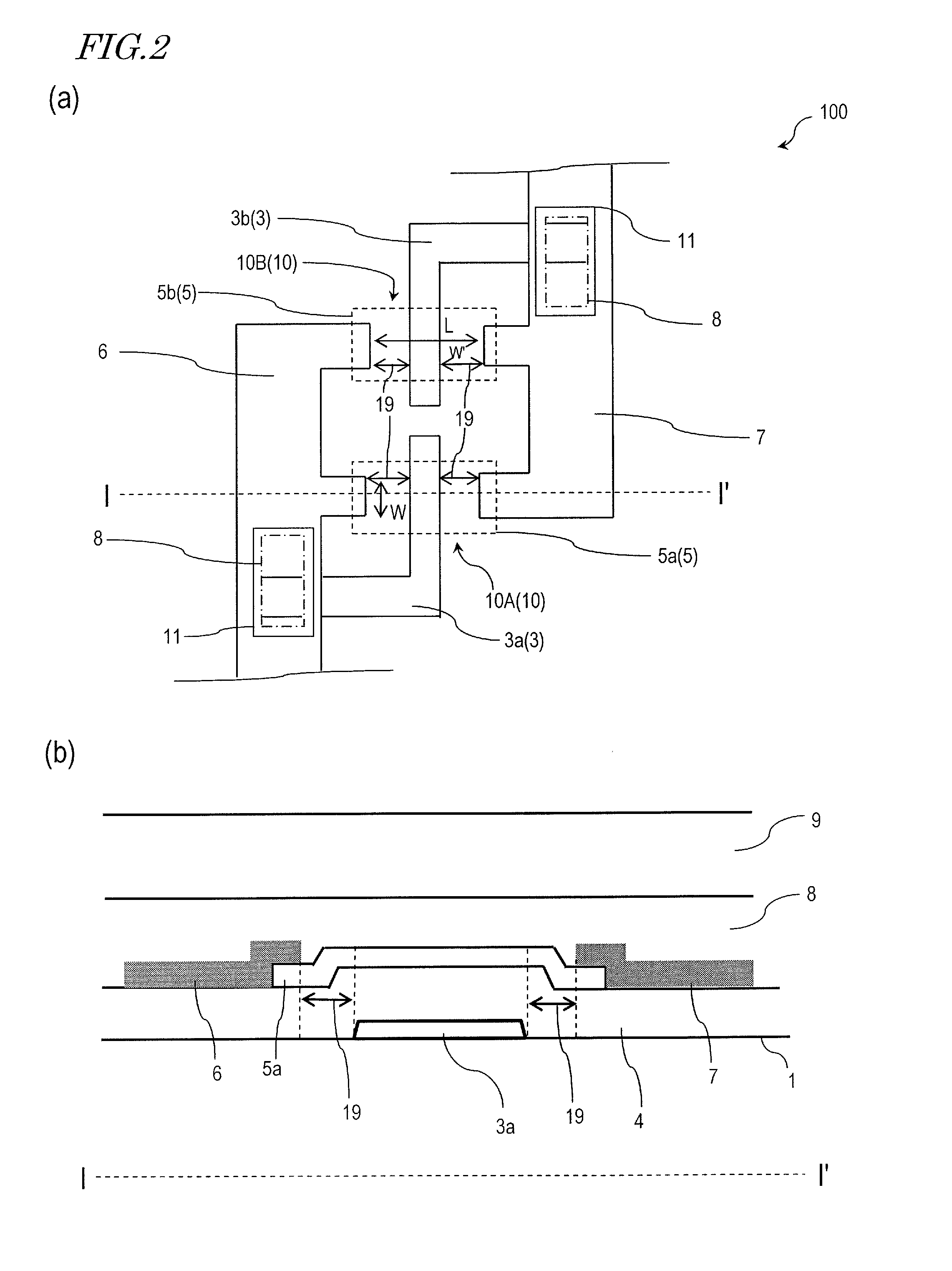
[0030]Hereinafter, with reference to FIG. 1 and FIG. 2, a semiconductor device 100 according to an embodiment of the present invention will be described. FIG. 1(a) is an equivalent circuit diagram of the semiconductor device 100, and FIG. 1(b) is a graph showing voltage (V)-current (I) characteristics of a diode element 10. FIG. 1(a) also shows liquid crystal capacitors 40.

[0031]As shown in FIG. 1(a), the semiconductor device 100 includes a plurality of gate lines 14 which are disposed in parallel to o...


PUM


Abstract

A semiconductor device (100) according to the present invention includes a diode element (10). The diode element (10) includes: a first electrode (3) made of the same electrically conductive film as a gate electrode of a thin film transistor; an oxide semiconductor layer (5); and a second electrode (6) and a third electrode (7) being made of the same electrically conductive film as a source electrode of the thin film transistor and being in contact with the oxide semiconductor layer (5). The oxide semiconductor layer (5) includes offset regions (19) respectively between the first electrode (3) and the second electrode (6) and between the first electrode (3) and the third electrode (7).

Description

TECHNICAL FIELD[0001]The present invention relates to a semiconductor device having a thin film transistor (TFT), and a display device including such a semiconductor device.[0002]BACKGROUND ART[0003]In recent years, there is vigorous development of[0004]TFTs (oxide semiconductor TFTs) in which an oxide semiconductor layer containing indium (In), zinc (Zn), gallium (Ga), or the like is used (e.g. Patent Documents 1 to 3). Since oxide semiconductor TFTs have high mobility characteristics, the display quality of a liquid crystal display device having oxide semiconductor TFTs is expected to be improved, for example.[0005]On the other hand, the fabrication process of a semiconductor device includes steps which are liable to static electricity. Static electricity may induce changes in characteristics or electrostatic discharge failures, thus resulting in a problem in that the production yield of semiconductor devices having the TFTs may be deteriorated.[0006]Deterioration in production yi...

Claims


Application Information

Patent Timeline
Patent Type & Authority Applications(United States)
IPC IPC(8): H01L27/12
CPCH01L27/1225H01L29/7869G02F1/136204G02F1/1365G02F2202/22G02F1/1368H01L27/1255H01L29/78621
Inventor HARA, YOSHIHITONAKATA, YUKINOBU
Owner SHARP KK
Why Eureka
Try Eureka