Area-efficient process-and-temperature-adaptive self-time scheme for performance and power improvement

a self-time scheme and temperature adaptation technology, applied in the field of integrated circuits, can solve the problems of conventional self-timing circuits triggering the sense amplifier too soon, self-timing circuits triggering the sense amplifier too late, etc., and achieve the effect of improving the timing performance of sense amplifiers

a self-time scheme and temperature adaptation technology, applied in the field of integrated circuits, can solve the problems of conventional self-timing circuits triggering the sense amplifier too soon, self-timing circuits triggering the sense amplifier too late, etc., and achieve the effect of improving the timing performance of sense amplifiers

US20150155021A1Inactive Publication Date: 2015-06-04AVAGO TECH INT SALES PTE LTD

Image

  • Area-efficient process-and-temperature-adaptive self-time scheme for performance and power improvement
  • Area-efficient process-and-temperature-adaptive self-time scheme for performance and power improvement
  • Area-efficient process-and-temperature-adaptive self-time scheme for performance and power improvement

Examples


Embodiment Construction

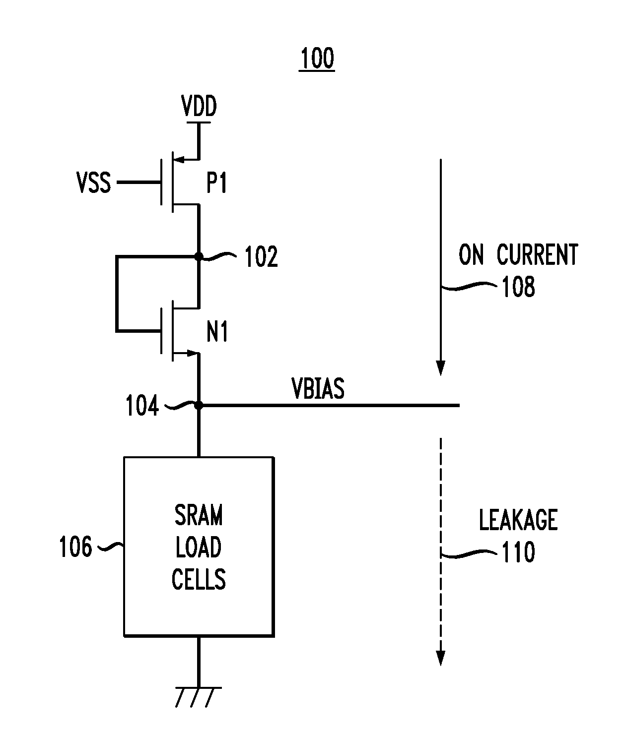
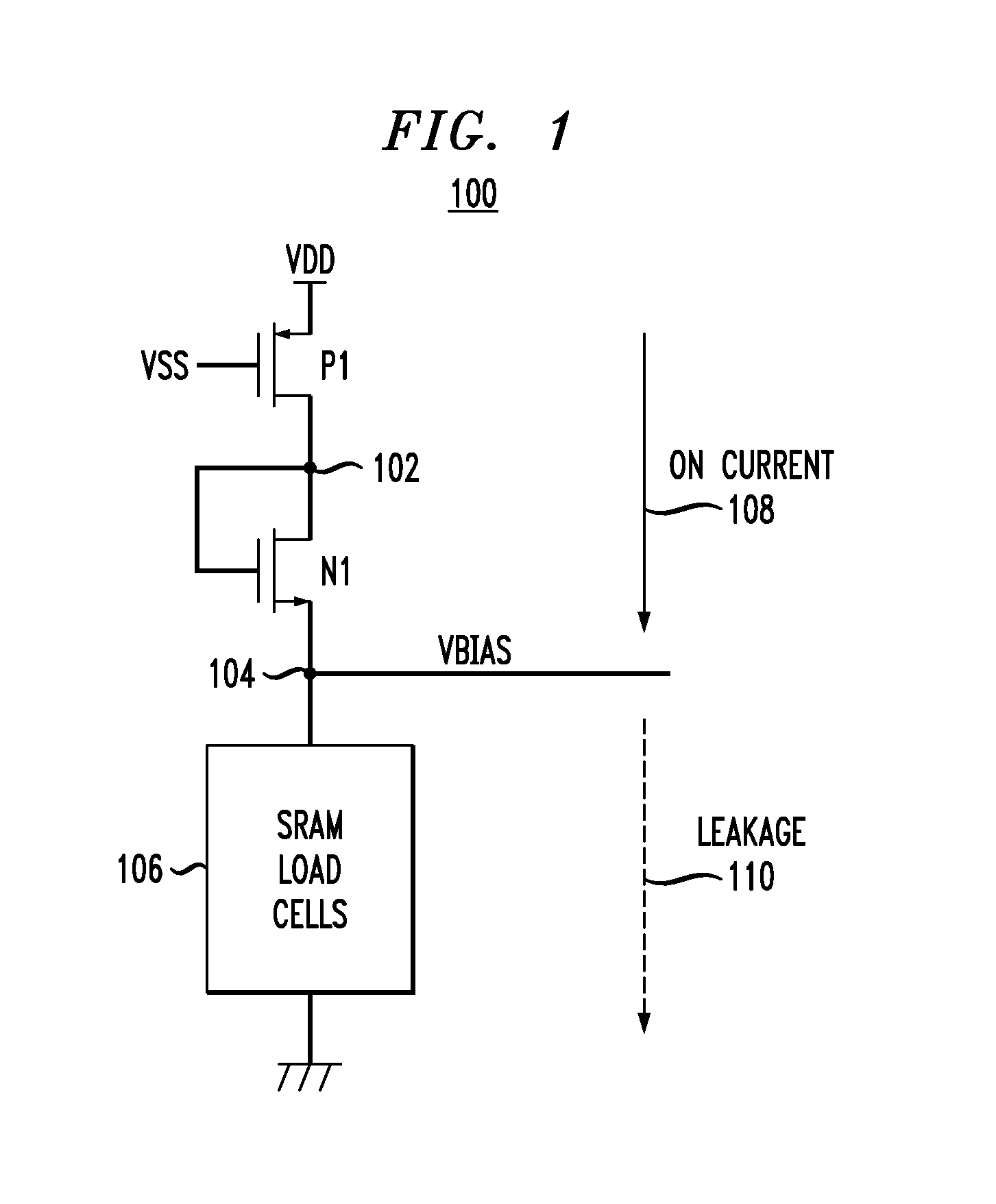
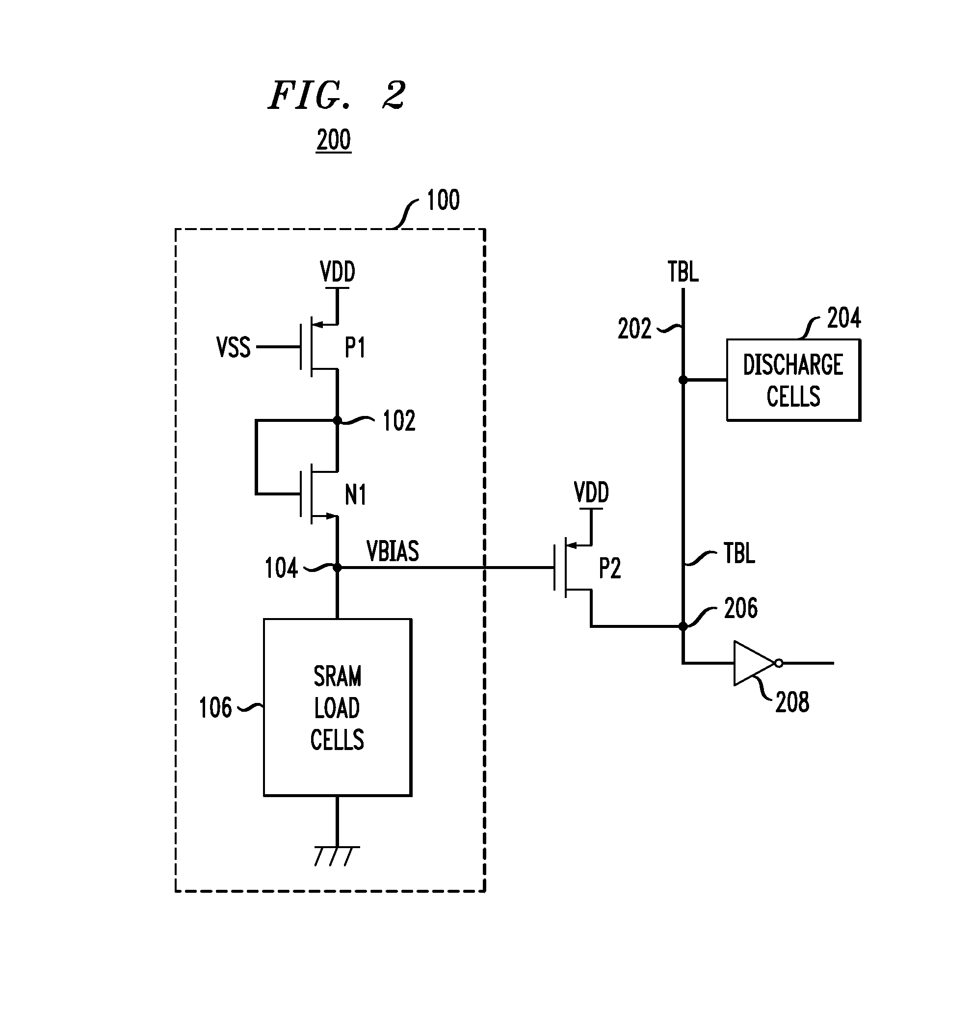
[0023]FIG. 1 depicts bias circuit 100, which comprises P-type transistor P1 having a source terminal connected to a first supply-voltage source (e.g., VDD), a gate terminal connected to a control-voltage source (e.g., supply-voltage source VSS), and a drain terminal connected to node 102. Bias circuit 100 further comprises N-type transistor N1 having a drain terminal connected to node 102, a gate terminal also connected to node 102, and a source terminal connected to node 104. One or more load cells 106 are connected either between node 104 and circuit ground or, alternatively, between node 104 and a second supply-voltage source (e.g., VSS).

[0024]Bias circuit 100 operates to produce a process-and-temperature-dependent bias signal VBIAS at node 104 in the following manner. The application of voltage VSS to the gate terminal of transistor P1 tends to cause the transistor to be conductive (or switched “on”). Because the gate and drain terminals of N-type transistor N1 are connected, tr...


PUM


Abstract

In certain embodiments, a method and apparatus for adjusting the timing of a sense-amplifier read operation in an SRAM integrated memory circuit to overcome process-and-temperature variations are disclosed. A charge-injection pull-up transistor is provided to adjust the rate at which a signal line (e.g., a tracking bit line (TBL) and / or a clock signal (e.g., GCLKB)) transitions from one voltage level to another voltage level. A process-and-temperature-dependent bias circuit is provided to control the charge-injection pull-up transistor. The bias circuit causes the charge-injection pull-up transistor to adjust the discharge rate or transition rate of the signal line to compensate for timing delays caused by process or temperature variations.

Description

CROSS-REFERENCE TO RELATED APPLICATION[0001]This application claims the benefit of Indian Patent Application No. 5594 / CHE / 2013 filed Dec. 4, 2013, the entire contents of which are incorporated herein by reference.BACKGROUND OF THE INVENTION[0002]1. Field of the Invention[0003]The present invention relates to integrated circuits, and, more specifically but not exclusively, to a bias circuit for adjusting timing or clock signals in memory circuits.[0004]2. Description of the Related Art[0005]Modern static random-access memory (SRAM) devices include one or more latching differential sense amplifiers that are designed to sense, amplify, and latch a differential bit-line signal from a memory cell. (See, e.g., U.S. Pat. Nos. 5,936,905; 6,738,296 B2; 7,623,400 B2; and 8,279,659 B2 and U.S. Patent Publication No. 2012 / 0195106 A1, the contents of all of which are hereby incorporated by reference.) The timing of the latch for each sense amplifier is determined by a self-timing pulse (also kno...

Claims


Application Information

Patent Timeline
04 Jun 2015
Publication
US20150155021A1
IPC
G11C7/22; G11C5/14; G11C7/08
CPC
G11C7/227; G11C5/14; G11C7/08; G11C7/04; G11C11/417; G11C29/026
Inventors
GOEL, ANKUR; RAI, DHARMENDRA KUMAR