Semiconductor memory device having a delay circuit for generating a read timing

a delay circuit and memory device technology, applied in the direction of pulse manipulation, pulse technique, instruments, etc., can solve the problems of excessive timing margin, new delay generation in the counter, and difficulty in determining the timing of data latches in large-scale/high-speed semiconductor devices

Inactive Publication Date: 2001-08-28
RENESAS ELECTRONICS CORP
View PDF3 Cites 61 Cited by
  • Summary
  • Abstract
  • Description
  • Claims
  • Application Information

AI Technical Summary

Benefits of technology

It is an object of the present invention to provide a delay circuit which is capable of generating an optimum delay time providing an optimum timing of the data latch in a large scale integrated semiconductor device such as a SRAM.

Problems solved by technology

It is generally difficult to determine the timing of data latch in a large-scale / high-speed semiconductor device such as a SRAM and an asynchronous semiconductor memory device.
This difficulty results in part from the timing difference generally involved between signals supplied from a large number of memory cells disposed at different positions.
In this case, however, the timing margin is excessively large to a memory cell which is located nearer than the recited memory cell.
A new delay is generated in the counter, however, when the counter converts the analog signal to a digital signal.
In the technique described in the literature, there is a problem in that an irregularity or fluctuation such as caused by the fabrication process or a temperature change prevents generation of an optical timing signal Vs.
In addition, there arises a similar problem if the waiting time is unstable before the delay time is changed based on the fundamental clock signal and the count in the counter.
Furthermore, the circuit scale of the memory device becomes large due to provision of the comparator and the counter.

Method used


Image

  • Semiconductor memory device having a delay circuit for generating a read timing
  • Semiconductor memory device having a delay circuit for generating a read timing
  • Semiconductor memory device having a delay circuit for generating a read timing

Examples


first embodiment

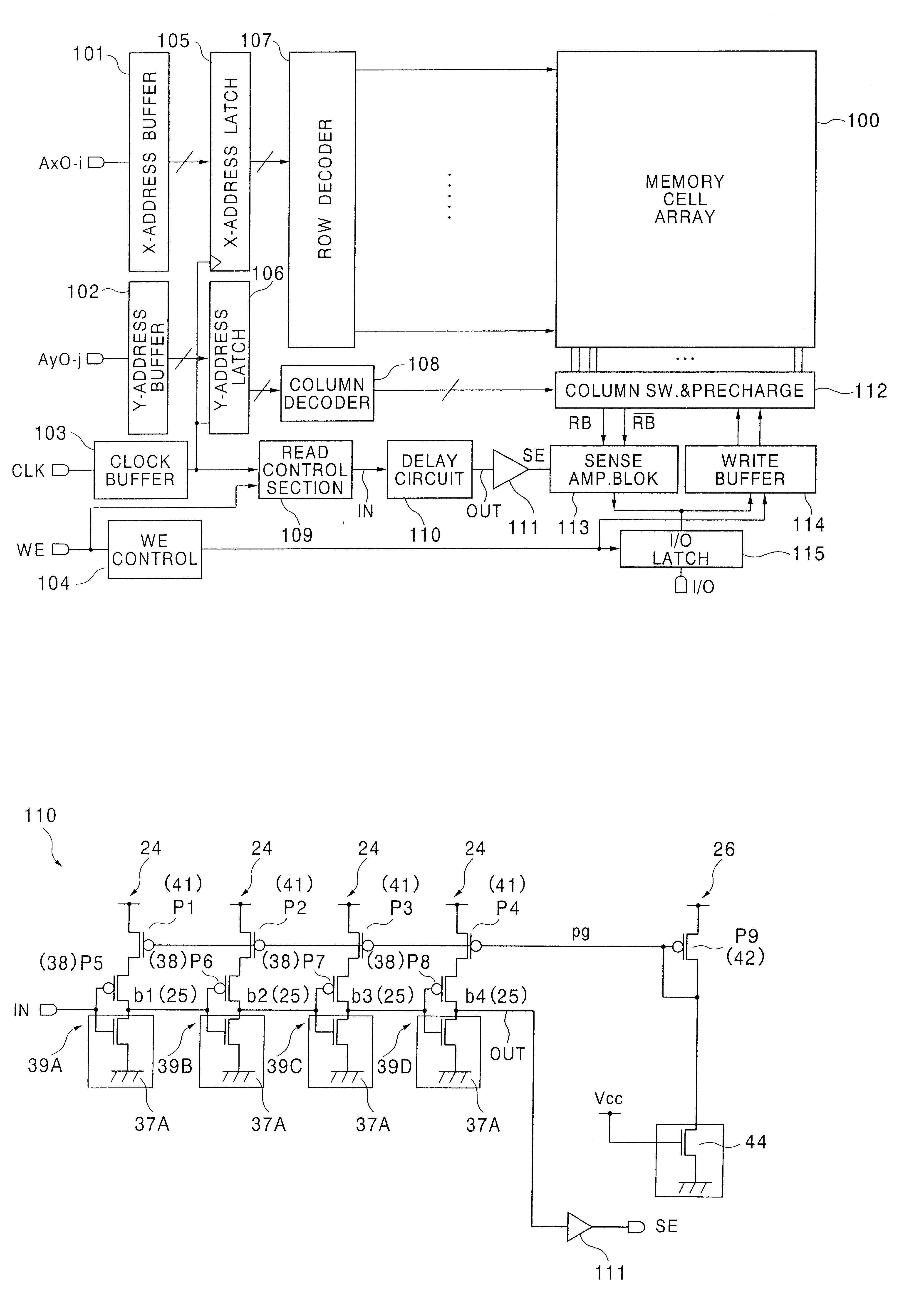
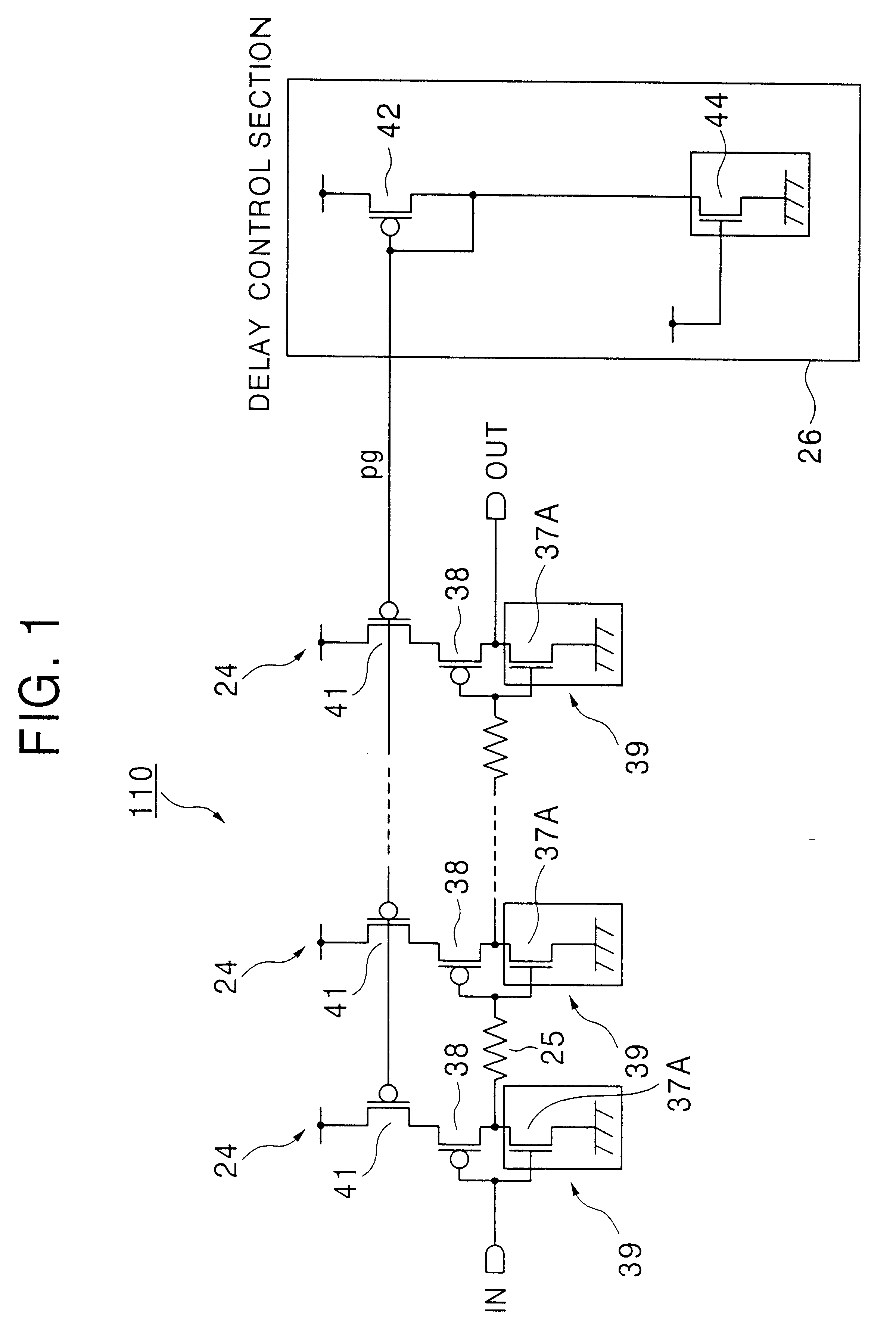
Referring to FIG. 1, a delay circuit 110 according to the present invention includes a plurality of cascaded inverters 39 each including a pMOSFET 38 and a nMOSFET 37A including a plurality of nMOSFET elements connected in parallel. The pMOSFET 38 and the nMOSFET 37A are connected in a complementary configuration between a source line and the ground line, with a pMOSFET 41 connected between the source line and the pMOSFET 38.

Each of the nMOSFET elements forming the nMOSFET 37A in the inverter 39 shown in FIG. 1 has a configuration similar to the configuration of nMOSFET transfer gates 205 and 206 in a memory cell 100a shown in FIGS. 3A and 3B.

The inverters 39 are cascaded via dummy bit lines 25, and afford a signal delay corresponding to the delay of a pair of bit lines bt and / bt associated with the memory cells 100a. The symbol" / " as used herein, such as in" / bt", means an inversion of the signal, such as"bt", succeeding the symbol " / ".

Due to the configuration of the nMOSFET 37A in...

second embodiment

Referring to FIG. 10, a delay circuit 110 in a semiconductor memory device according to the present invention is similar to the delay circuit of FIG. 8 except that a pMOSFET P10 (43) is provided in series with the pMOSFET P9 (42) in the delay control section 26 in the present embodiment. The pMOSFET 43 has a configuration similar to the configuration of the pMOSFETs 38, and the gate of the pMOSFET 43 is connected to the ground. The provision of the pMOSFET 43 improves the accuracy of the current ratio in the current mirror.

fourth embodiment

Referring to FIG. 11, a delay circuit in a semiconductor memory device according to the present invention is similar to the delay circuit of FIG. 10 except that the gate of the pMOSFET 43 is finely controlled to obtain an optimum current in the delay control section 26.


PUM


Abstract

A delay circuit in a semiconductor memory device generates a sense amplifier enable signal having a delay time with respect to the timing of selection of one of memory cells. The delay time corresponds to the largest read time for the memory cell located at the most distant position and has an irregularity reflecting an irregularity in threshold voltage of nMOSFET transfer gates in each memory cell, which affects the read time. An optimum timing for the sense amplifier enable signal can be obtained by the delay circuit irrespective of the irregularity in the threshold voltage of the nMOSFET transfer gates.

Description

FIELD OF THE INVENTIONThe present invention relates to a semiconductor memory device having a delay circuit for generating a read timing of a sense amplifier in the memory device. The present invention also relates to a general semiconductor device having such a delay circuit.DESCRIPTION OF A RELATED ARTIt is generally difficult to determine the timing of data latch in a large-scale / high-speed semiconductor device such as a SRAM and an asynchronous semiconductor memory device. This difficulty results in part from the timing difference generally involved between signals supplied from a large number of memory cells disposed at different positions. It is proposed in JP-A-6-170998, for example, that data be latched by a sense amplifier in a semiconductor memory device based on the timing of the data having a largest time delay.More specifically, the asynchronous memory device described in the publication has a plurality of dummy memory circuits each having a delay characteristic similar...

Claims


Application Information

Patent Timeline
Patent Type & Authority Patents(United States)
IPC IPC(8): G11C7/22G11C7/00G11C7/06G11C11/419G11C11/417G11C8/00G11C11/4076G11C11/413H01L21/8244H01L27/10H01L27/11H03K5/13H03K19/0948
CPCG11C7/06G11C7/22G11C11/419H03K5/133G11C11/417H03K2005/00202G11C8/00
Inventor NAKAGAWA, ATSUSHITAKAHASHI, HIROYUKI
Owner RENESAS ELECTRONICS CORP
Why Eureka
Try Eureka