Atomic layer deposition of silicon carbon nitride based materials

a technology of silicon carbon nitride and atomic layer deposition, which is applied in the direction of chemical vapor deposition coating, coating, metallic material coating process, etc., can solve the problems of low conformality and/or undesired low film quality inside three-dimensional structures, low conformality and/or reduced film quality, and the effect of reducing the thickness of the film

Active Publication Date: 2015-06-11
ASM IP HLDG BV
View PDF6 Cites 353 Cited by
  • Summary
  • Abstract
  • Description
  • Claims
  • Application Information

AI Technical Summary

Problems solved by technology

Deposition of silicon nitride based films having desired characteristics by atomic layer deposition (ALD) processes using reduced thermal budgets can be difficult (e.g., such as at reduced temperatures, including at temperatures of less than about 600° C.).
Silicon nitride based films deposited by conventional processes (e.g., silicon nitride based film deposited using plasma enhanced ALD (PEALD)) performed at reduced temperatures may result in films having undesirably low conformality and/or undesirably low film quality insi

Method used


Image

  • Atomic layer deposition of silicon carbon nitride based materials
  • Atomic layer deposition of silicon carbon nitride based materials
  • Atomic layer deposition of silicon carbon nitride based materials

Examples


Embodiment Construction

[0027]Although certain embodiments and examples are described below, those of skill in the art will appreciate that the invention extends beyond the specifically disclosed embodiments and / or uses and includes obvious modifications and equivalents thereof. Thus, it is intended that the scope of the invention herein disclosed should not be limited by any particular embodiments described below.

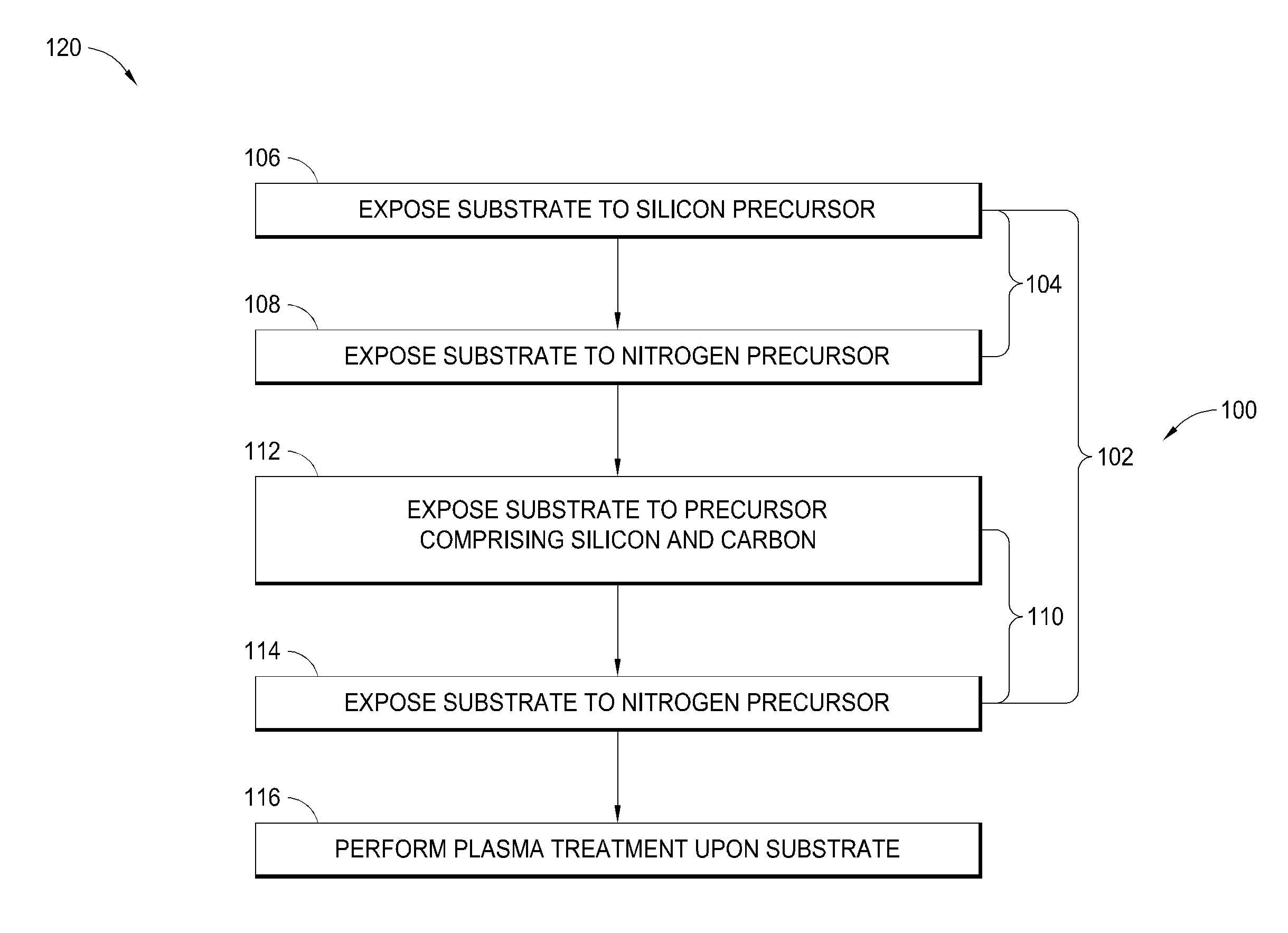
[0028]In some embodiments, a process of fabricating a silicon nitride based material containing carbon, or a silicon carbon nitride (SiCN) film, having desirable characteristics (e.g., desired conformality and / or reduced wet etch rate in dilute aqueous hydrofluoric acid solution) can include a thermal atomic layer deposition (ALD) process performed at reduced temperatures (e.g., at less than about 600° C., including about 300° C. to about 600° C., and about 400° C. to about 500° C.). In some embodiments, addition of carbon into a silicon nitride film can advantageously provide a film having desir...


PUM

PropertyMeasurementUnit
Timeaaaaaaaaaa
Percent by massaaaaaaaaaa
Etch rateaaaaaaaaaa

Abstract

A process for depositing a silicon carbon nitride film on a substrate can include a plurality of complete deposition cycles, each complete deposition cycle having a SiN sub-cycle and a SiCN sub-cycle. The SiN sub-cycle can include alternately and sequentially contacting the substrate with a silicon precursor and a SiN sub-cycle nitrogen precursor. The SiCN sub-cycle can include alternately and sequentially contacting the substrate with carbon-containing precursor and a SiCN sub-cycle nitrogen precursor. The SiN sub-cycle and the SiCN sub-cycle can include atomic layer deposition (ALD). The process for depositing the silicon carbon nitride film can include a plasma treatment. The plasma treatment can follow a completed plurality of complete deposition cycles.

Description

REFERENCE TO RELATED APPLICATIONS[0001]Any and all applications for which a foreign or domestic priority claim is identified in the Application Data Sheet as filed with the present application are hereby incorporated by reference under 37 CFR 1.57.BACKGROUND[0002]1. Field[0003]The present disclosure relates generally to the field of semiconductor device manufacturing and, more particularly, to deposition of silicon nitride based films.[0004]2. Description of the Related Art[0005]As the physical geometry of semiconductor devices shrinks, deposition processes for forming silicon nitride based films on three-dimensional structures having high aspect ratios is desired. Additionally, it is desirable to be able to deposit silicon nitride based films that demonstrate an advantageous etch selectivity with respect one or more other materials in the formation of a semiconductor device, and / or a desirable etch rate in a dry etch and / or wet etch process.[0006]Deposition of silicon nitride based...

Claims


Application Information

Patent Timeline
IPC IPC(8): H01L21/02
CPCH01L21/0234H01L21/02211H01L21/0228H01L21/02167H01L21/31111C23C16/30C23C16/45553H01L21/02208
Inventor PORE, VILJAMI
Owner ASM IP HLDG BV
Why Eureka
Try Eureka