Low temperature plasma enhanced chemical vapor deposition of conformal silicon carbon nitride and silicon nitride films

Active Publication Date: 2013-07-18
APPLIED MATERIALS INC
View PDF0 Cites 47 Cited by
  • Summary
  • Abstract
  • Description
  • Claims
  • Application Information

AI Technical Summary

Benefits of technology

[0009]The present invention generally provides methods and processes for forming a silicon nitride layer on a substrate. In one embodiment, a method of forming a silicon nitride layer includes performing a deposition cycle including flowing a processing gas mixture into a processing chamber having a substrate therein, wherein the processing gas mixture comprises precursor gas molecules having labile silicon to nitrogen, silicon to carbon, or nitrogen to carbon bonds, activating the precursor gas at a temperature between about 20° C. to about 480° C. by preferentially breaking labile bonds to provide one or more reaction sites along a precursor gas molecule, forming a precursor material layer on the substrate, wherein the activated precursor gas molecules bond with a surface on the substrate at the one or more reaction sites, and performing a plasma treatment process on the precursor material layer to form a conformal silicon nitride layer.
[0010]In another embodiment, a method of forming a silicon nitride layer includes flowing a processing gas mixture into a processing chamber having a substrate therein, wherein the processing gas mixture comprises precursor gas molecules having labile silicon to nitrogen, silicon to carbon, or nitrogen to carbon bonds, generating a plasma in the processing chamber at an RF power density from about 0.01 W/cm2 to about 40 W/cm2 and at a temperature between about 20° C. to about 480° C. to activate the precursor gas by preferentially breaking labile bonds to provide one or more reaction sites along a precursor gas molecule, forming a precursor material layer on the substrate, wherein the activated precursor gas molecules bond with a surface on the substrate at the one or more reaction sites, and performing a plasma treatment process on the precursor material layer to form a conformal silicon nitride layer and control the amount of carbon in the

Problems solved by technology

The drawbacks, however, include a high temperature requirement (typically greater than 400° C.) and few capabilities to engineer film compositions and properties for different applications.
Alternatively, conventional silane-based plasma enhanced chemical vapor deposition (PE-CV

Method used


Image

  • Low temperature plasma enhanced chemical vapor deposition of conformal silicon carbon nitride and silicon nitride films
  • Low temperature plasma enhanced chemical vapor deposition of conformal silicon carbon nitride and silicon nitride films
  • Low temperature plasma enhanced chemical vapor deposition of conformal silicon carbon nitride and silicon nitride films

Examples


example 1

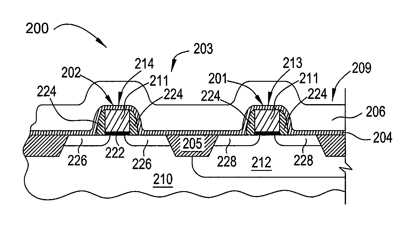
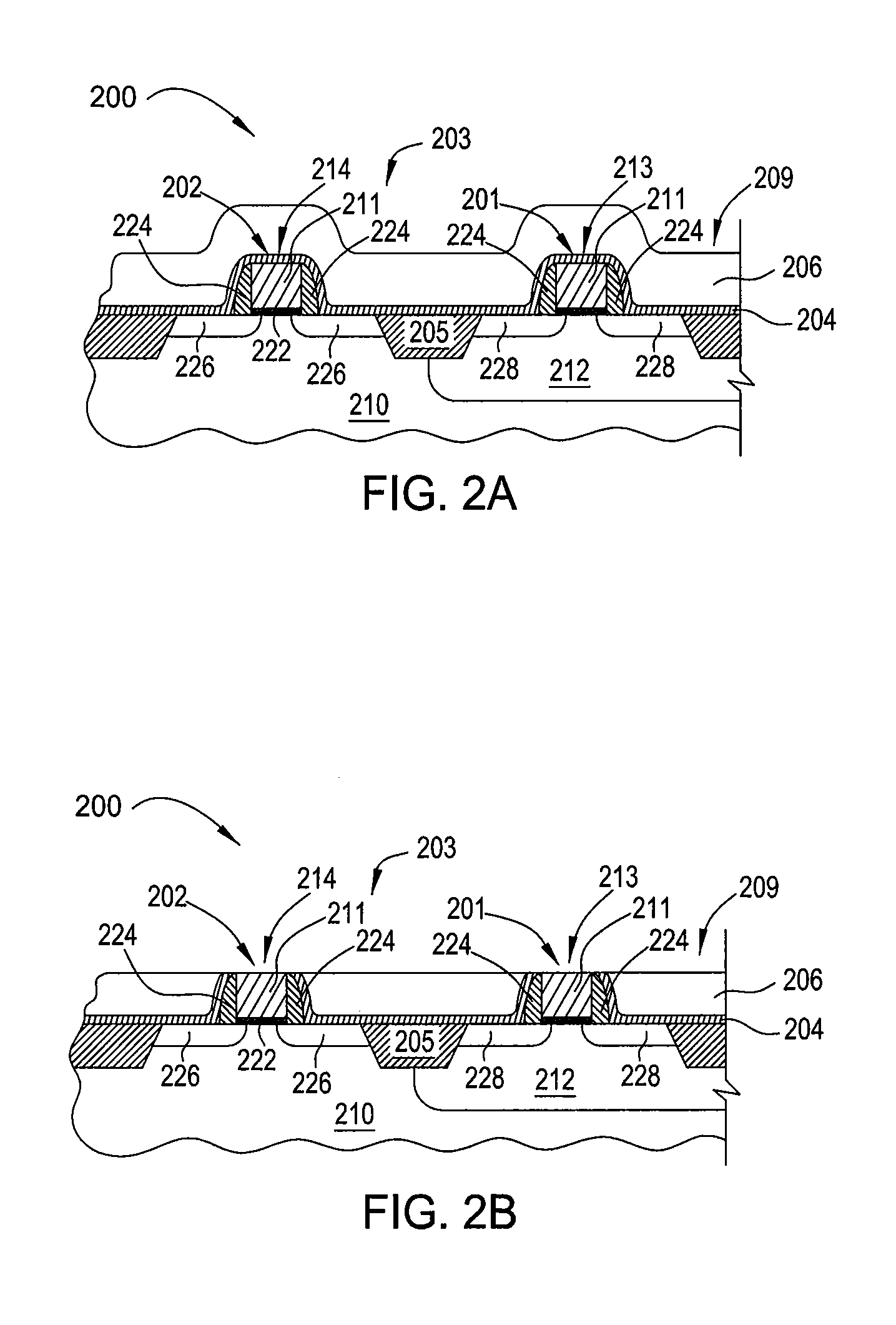
[0062]A conformal silicon nitride layer may be deposited on a 300 mm substrate by a PECVD process. The substrate and the substrate pedestal were heated to a temperature of about 200° C. The substrate was exposed to a hydrocarbon precursor having silicon and nitrogen, C6H21N3Si3 (HMCTZ) and a He carrier gas under plasma conditions. The deposition plasma was generated at 50 watts for 10 seconds. The precursor gas had a flow rate of about 1000 mg / min. After forming a precursor material layer, the precursor gas flow was stopped and the substrate exposed to a plasma treatment process including H2 gas for 10 seconds. The plasma treatment gas had a flow rate of about 5 slm. The treatment plasma was generated at 500 watts for 10 seconds. The silicon nitride material was deposited on the substrate to a final thickness of about 500 Å by 100 cycles of about 5 Å per cycle. The composition analysis of the conformal silicon nitride material provided conformality of 95% and PLE of 5%, and a carbon...

example 2

[0063]A conformal silicon nitride layer may be deposited on a 300 mm substrate by a PECVD process. The substrate and the substrate pedestal were heated to a temperature of about 200° C. The substrate was exposed to a hydrocarbon precursor having silicon and nitrogen, C6H21N3Si3 (HMCTZ) and a He carrier gas under a plasma conditions. The deposition plasma was generated at 50 watts for 10 seconds. The precursor gas had a flow rate of about 1000 mg / min. After forming a precursor material layer, the precursor gas flow was stopped and the substrate exposed to a plasma treatment process including NH3 gas for 15 seconds. The plasma treatment gas had a flow rate of about 10 slm. The treatment plasma was generated at 500 watts for 15 seconds. The silicon nitride material was deposited on the substrate to a final thickness of about 450 Å by 100 cycles of about 4.5 Å per cycle and the composition analysis showed <2% carbon content and conformality of greater than 90% and PLE of 5%.

[0064]A UV c...


PUM


Abstract

Methods and apparatus for forming conformal silicon nitride films at low temperatures on a substrate are provided. The methods of forming a silicon nitride layer include performing a deposition cycle including flowing a processing gas mixture into a processing chamber having a substrate therein, wherein the processing gas mixture comprises precursor gas molecules having labile silicon to nitrogen, silicon to carbon, or nitrogen to carbon bonds, activating the precursor gas at a temperature between about 20° C. to about 480° C. by preferentially breaking labile bonds to provide one or more reaction sites along a precursor gas molecule, forming a precursor material layer on the substrate, wherein the activated precursor gas molecules bond with a surface on the substrate at the one or more reaction sites, and performing a plasma treatment process on the precursor material layer to form a conformal silicon nitride layer.

Description

BACKGROUND OF THE INVENTION[0001]1. Field of the Invention[0002]Embodiments of the present invention generally relate to methods and processes for forming conformal silicon nitride films, including doped silicon nitride films, at low temperatures.[0003]2. Description of the Related Art[0004]The electronic device industry and the semiconductor industry continue to strive for larger production yields while increasing the uniformity of layers deposited on substrates having increasingly larger surface areas. These same factors in combination with new materials also provide higher integration of circuits per unit area on the substrate. As circuit integration increases, the need for greater uniformity and process control regarding layer characteristics rises.[0005]For example, ultra-large-scale integrated (ULSI) circuits typically include more than one million transistors that are formed on a semiconductor substrate and which cooperate to perform various functions within an electronic dev...

Claims


Application Information

Patent Timeline
IPC IPC(8): H01L21/318
CPCC23C16/345C23C16/56H01L21/823807H01L29/7843H01L21/02348H01L21/0217H01L21/02222H01L21/02274H01L21/0234H01L21/02167H01L21/02208H01L21/0228H01L21/324
Inventor NGUYEN, VICTORBALSEANU, MIHAELAXIA, LI-QUNWITTY, DEREK R.
Owner APPLIED MATERIALS INC
Why Eureka
Try Eureka