Non-volatile memory device including flexible NANO floating gate and method for fabricating the same
a technology of floating gate and non-volatile memory, which is applied in the direction of semiconductor devices, material nanotechnology, electrical devices, etc., can solve the problems of increasing the variability of the threshold voltage of the device, requiring a great deal of power consumption, and loss of stored data, etc., to achieve excellent operation stability, low power consumption, and reliability.
- Summary
- Abstract
- Description
- Claims
- Application Information
AI Technical Summary
Benefits of technology
Problems solved by technology
Method used
Image

Examples
first embodiment
[0075][Improved Nano Floating Gate and Method for Forming the Same in Accordance with the Present Invention]
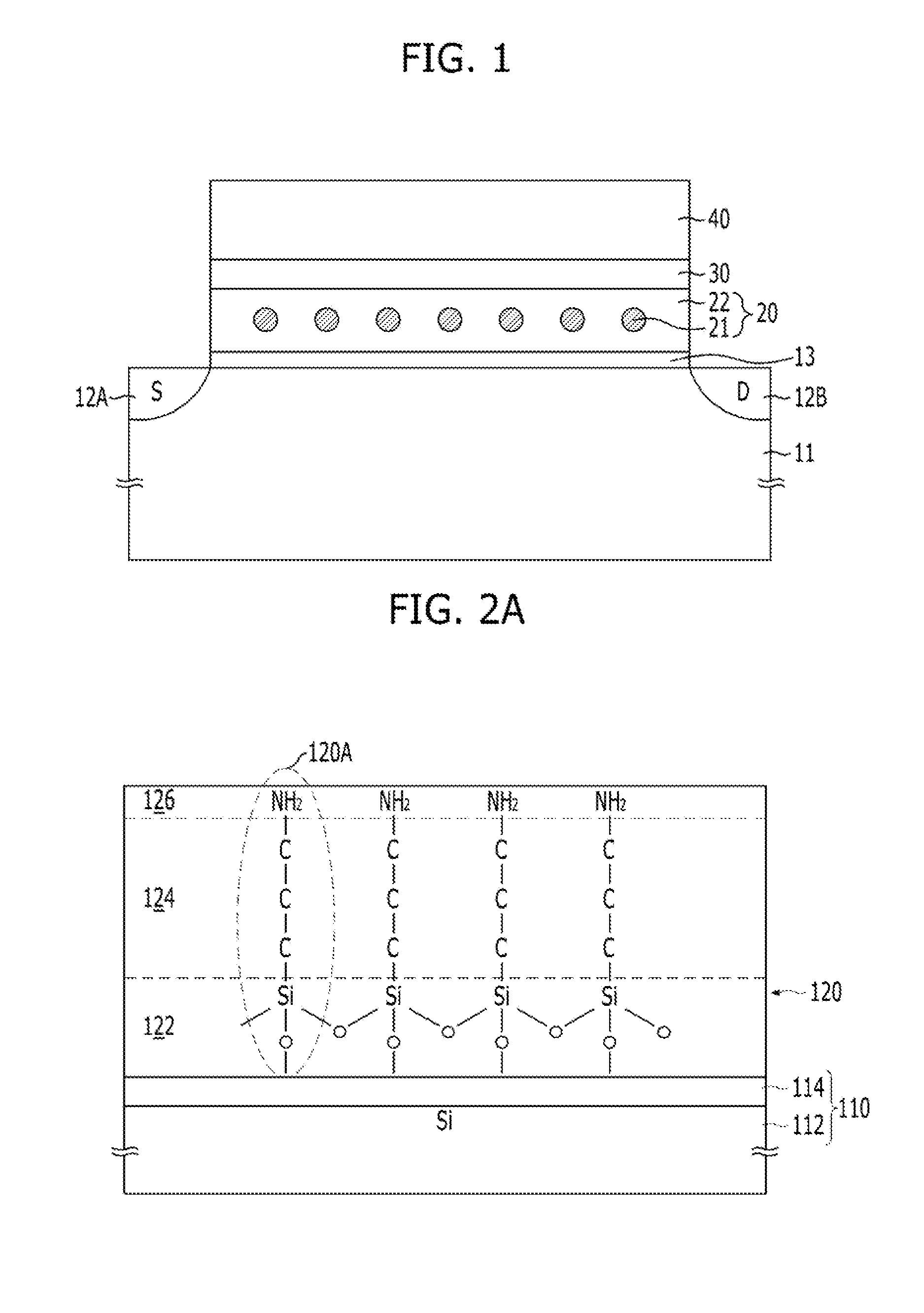
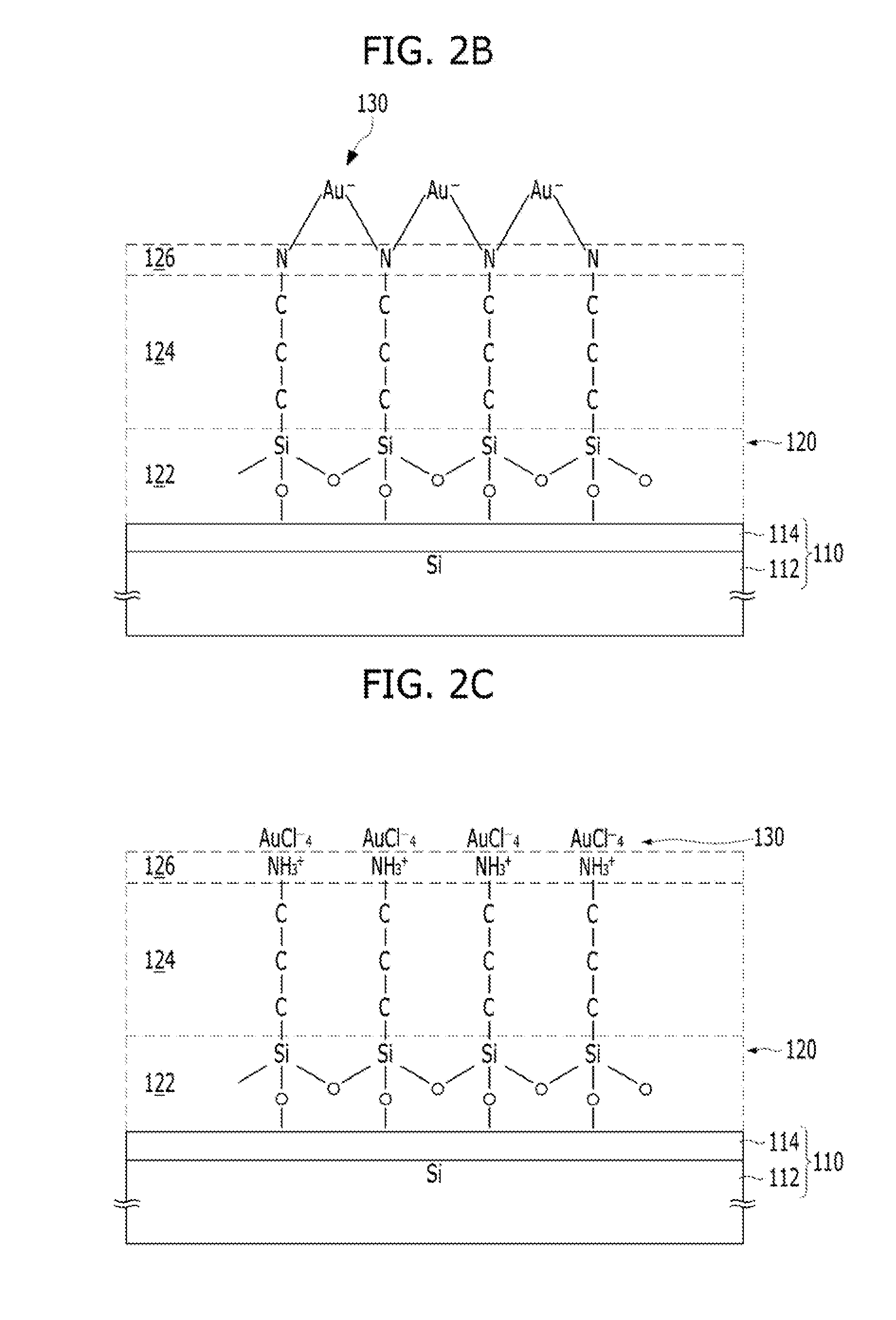
[0076]FIGS. 2A to 2E are cross-sectional views illustrating a method for forming the nano floating gate in accordance with a first embodiment of the present disclosure.
[0077]In accordance with the first embodiment of the present disclosure, a method for fabricating a non-volatile memory device including a nano floating gate may include bonding linkers 120A to a substrate 110 (see FIG. 2A); bonding metal ions 130 to the linkers 120A (see FIGS. 2B and 2C); and forming the metal ions 130 into metallic nanoparticles 140 by applying energy (see FIG. 2D). Also, the method for fabricating a non-volatile memory device including a nano floating gate may further include supplying a dielectric organic material 150 to the structure including the metallic nanoparticles (see FIG. 2E). Also, the method for fabricating a non-volatile memory device including a nano floating gate may further in...
second embodiment
[0184][Improved Nano Floating Gate and Method for Forming the Same in Accordance with the Present Invention]
[0185]FIGS. 3A to 3D are cross-sectional views describing a method for forming a nano floating gate in accordance with a second embodiment of the present disclosure.
[0186]The method for fabricating the nano floating gate in accordance with the second embodiment of the present disclosure may include forming dielectric material particle supporters 222 bonded to linkers 224 on the surface of a substrate 210 (refer to FIG. 3A), bonding metal ions 230 to the linkers 224 (refer to FIG. 3B), and transforming the metal ions 230 into metallic nanoparticles 240 by applying energy to the metallic nanoparticles 240 (refer to FIG. 3C). Also, the method may include supplying a dielectric organic material 250 to the structure where the metallic nanoparticles 240 are formed (refer to FIG. 3D). The method may further include supplying one or multiple kinds of organic surfactant before or durin...
PUM
 Abstract
Description
Claims
Application Information