Semiconductor device and fabrication method

a semiconductor and semiconductor technology, applied in the direction of semiconductor/solid-state device details, semiconductor devices, electrical apparatus, etc., can solve the problems of slow operating speed, parasitic capacitance problems of semiconductor devices formed by conventional methods, and affect the operating speed of semiconductor chips

Active Publication Date: 2015-07-02
SEMICON MFG INT (SHANGHAI) CORP
View PDF4 Cites 0 Cited by
  • Summary
  • Abstract
  • Description
  • Claims
  • Application Information

AI Technical Summary

Problems solved by technology

Parasitic capacitance may affect RC delay effect of the semiconductor devices and thus affect operating speed of the semiconductor chip along with reliability of the semiconductor devices in the semiconductor chip.
Howeve

Method used


Image

  • Semiconductor device and fabrication method
  • Semiconductor device and fabrication method
  • Semiconductor device and fabrication method

Examples


Embodiment Construction

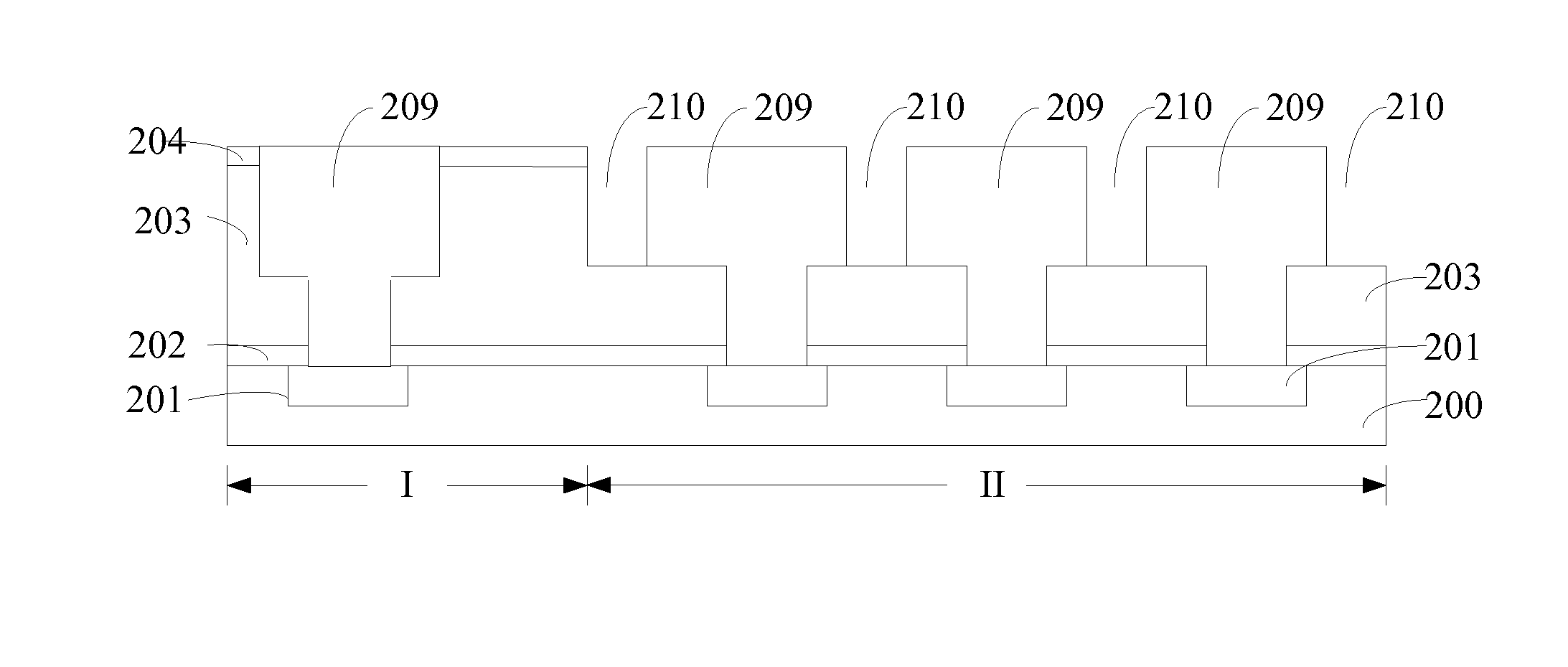
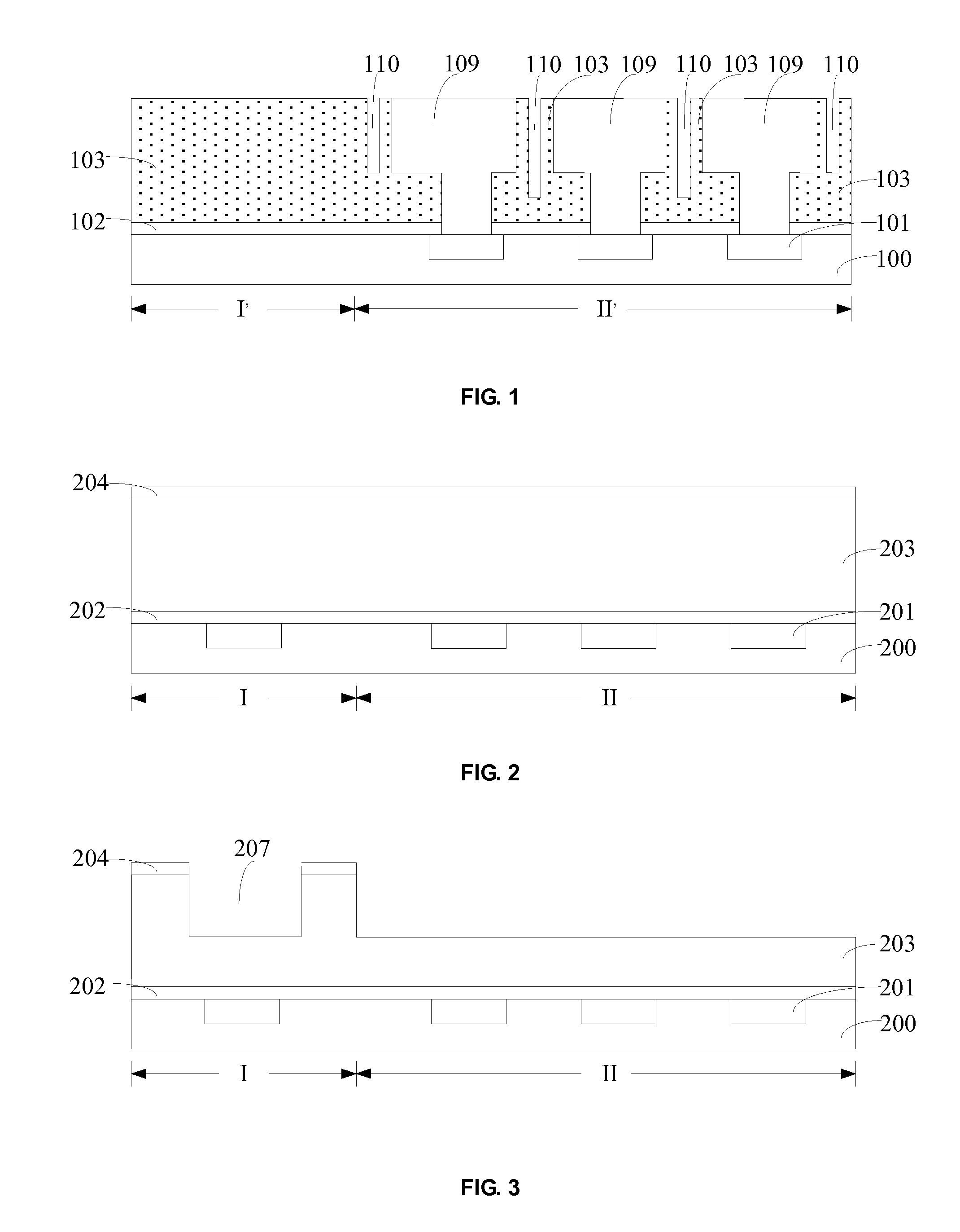
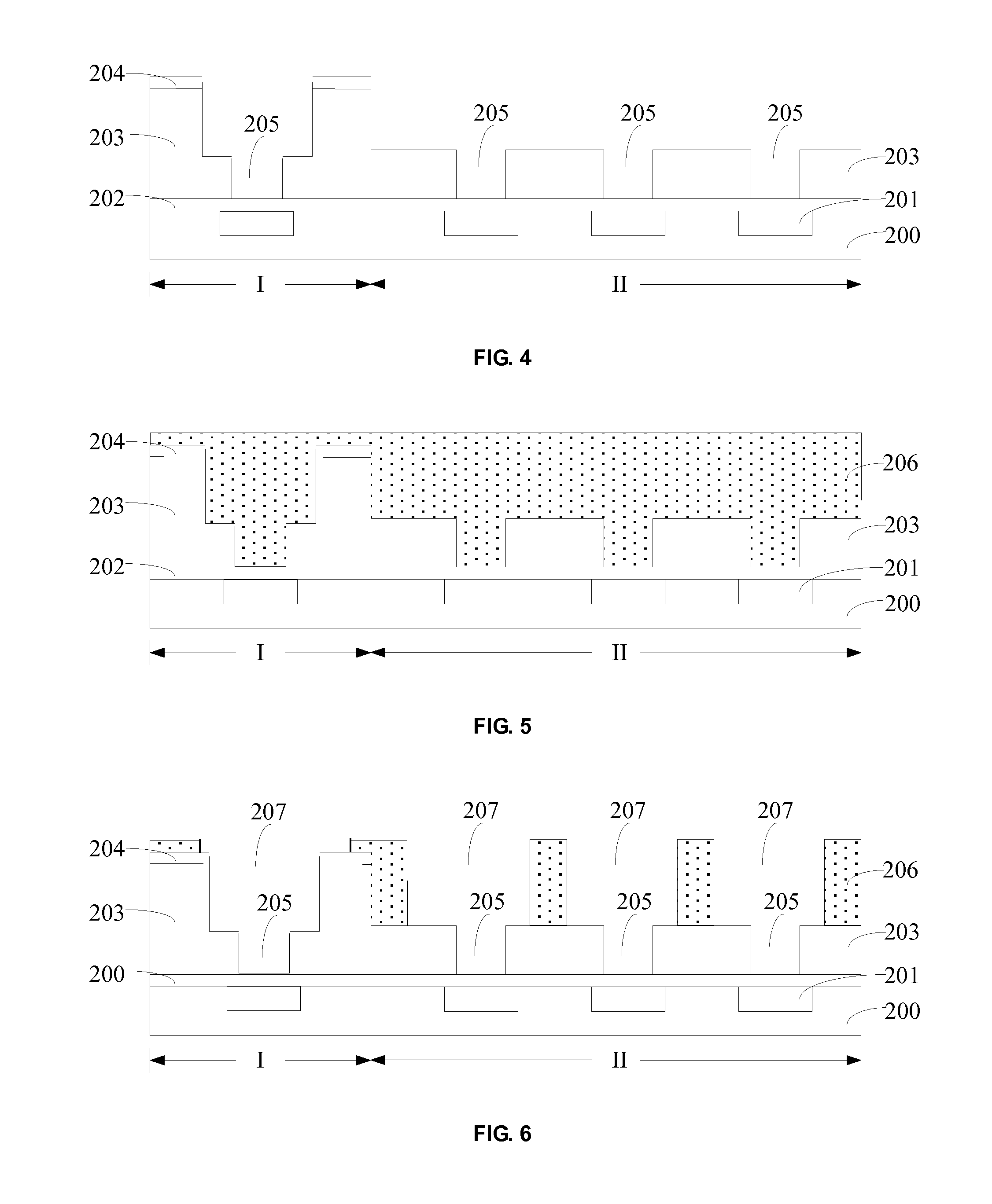
[0016]Reference will now be made in detail to exemplary embodiments of the disclosure, which are illustrated in the accompanying drawings. Wherever possible, the same reference numbers will be used throughout the drawings to refer to the same or like parts.

[0017]Semiconductor devices formed by conventional methods may have parasitic capacitance problems such as RC delay effects, which may cause slow operating speed and poor reliability of the semiconductor devices. Parasitic capacitance can be proportional to dielectric constant k of a semiconductor device. Lowering the k value of an interlayer dielectric layer and / or a dielectric layer between metal layers may reduce parasitic capacitance of the semiconductor device. Ideally, the dielectric constant k of the interlayer dielectric layer and the dielectric layer between metal layers can be reduced to about 1.0, which is the dielectric constant of vacuum. The dielectric constant of air is about 1.001, close to that of the vacuum.

[0018...


PUM


Abstract

Semiconductor devices and fabrication methods are provided. First metal layers are provided in a substrate including a first region and a second region. An interlayer dielectric (ILD) layer formed over the substrate includes a top surface in the second region coplanar with a bottom of a trench in the ILD layer in the first region. Through-holes are formed in the ILD layer. A polymer layer fills the through-holes and the trench in ILD layer and covers top surface of ILD layer in both regions. The polymer layer is exposed and developed to form vias, each including an upper via in the polymer layer and a lower via in ILD layer. A second metal layer is formed to fill each via on a corresponding first metal layer in both regions. The polymer layer between adjacent second metal layers is removed to form air gaps in the second region.

Description

CROSS-REFERENCES TO RELATED APPLICATIONS[0001]This application claims priority to Chinese Patent Application No. CN201310739057.9, filed on Dec. 27, 2013, the entire content of which is incorporated herein by reference.FIELD OF THE DISCLOSURE[0002]The present disclosure relates to the field of semiconductor manufacturing technology and, more particularly, relates to semiconductor devices and fabrication methods.BACKGROUND[0003]With rapid development of semiconductor manufacturing technology, semiconductor chips are manufactured with high degree of integration to provide fast computing speed, great data storage capacity, and more functions. High integration degree of a semiconductor chip can provide semiconductor devices in the semiconductor chip with small critical dimensions (CDs).[0004]When CDs of semiconductor devices are increasingly smaller, distance between adjacent interconnect structures become smaller. Consequently, capacitance between adjacent interconnect structures incre...

Claims


Application Information

Patent Timeline
IPC IPC(8): H01L21/768H01L23/48
CPCH01L21/7682H01L23/481H01L21/76843H01L21/76802H01L21/76828H01L2221/1042H01L2924/0002H01L23/5222H01L23/53295H01L21/76808H01L2924/00
Inventor WANG, XINPENGBU, WEIHAI
Owner SEMICON MFG INT (SHANGHAI) CORP
Why Eureka
Try Eureka