Semiconductor device and method for driving the same

a technology of magnetic field and magnetic field, applied in the direction of magnetic field/solid-state device details, digital storage, instruments, etc., can solve the problems of incorrect value reading out, difficult to determine a potential in reading data,

Active Publication Date: 2015-07-02
SEMICON ENERGY LAB CO LTD
View PDF2 Cites 33 Cited by
  • Summary
  • Abstract
  • Description
  • Claims
  • Application Information

AI Technical Summary

Benefits of technology

[0017]One embodiment of the present invention can provide e a novel semiconductor device, a semiconductor device where multilevel data can be written and read, or a method for driving a semiconductor device where multilevel data can be written and read.

Problems solved by technology

Thus, determining a potential in reading data becomes difficult, and an incorrect value might be read out.

Method used


Image

  • Semiconductor device and method for driving the same
  • Semiconductor device and method for driving the same
  • Semiconductor device and method for driving the same

Examples


embodiment 1

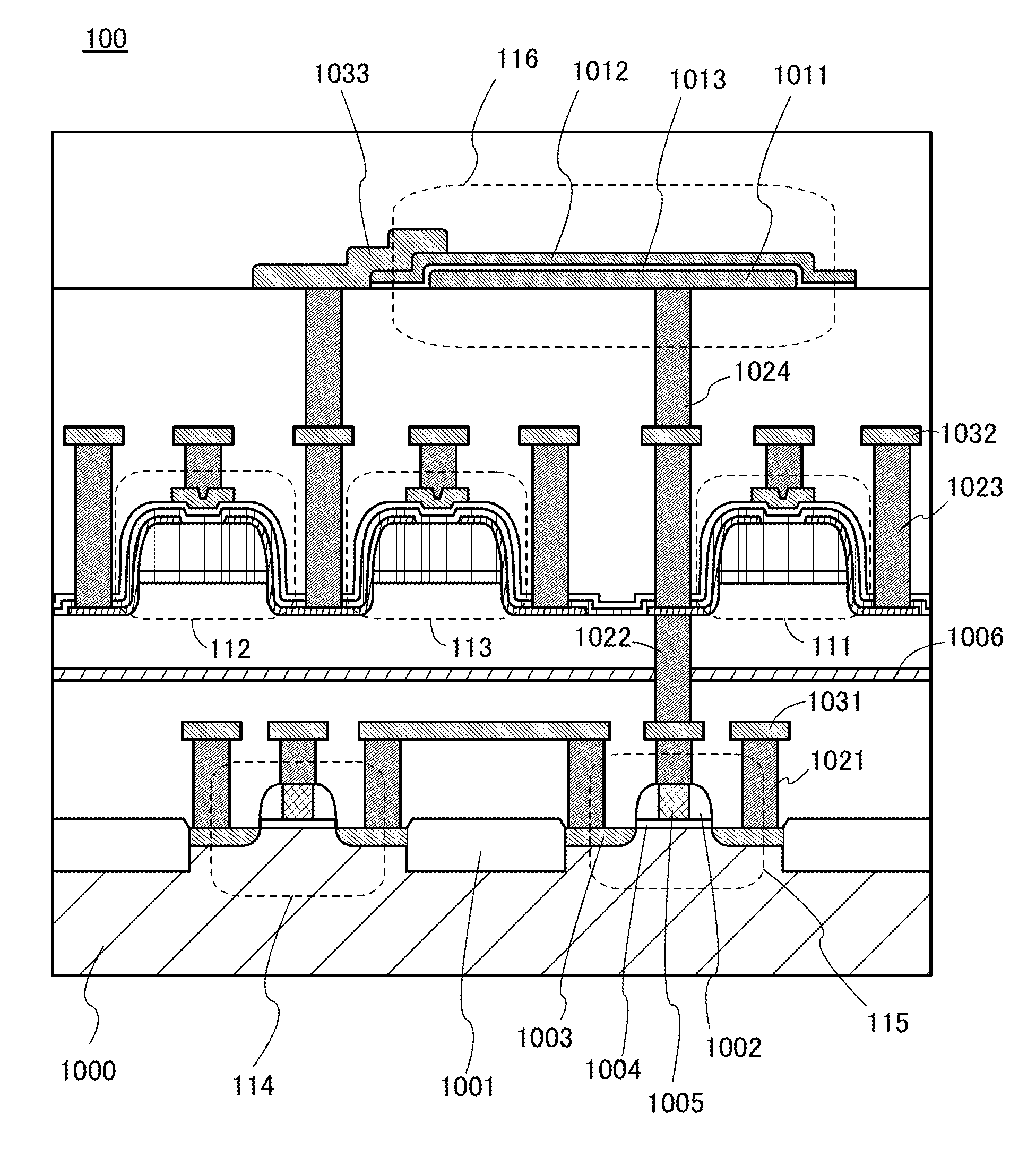
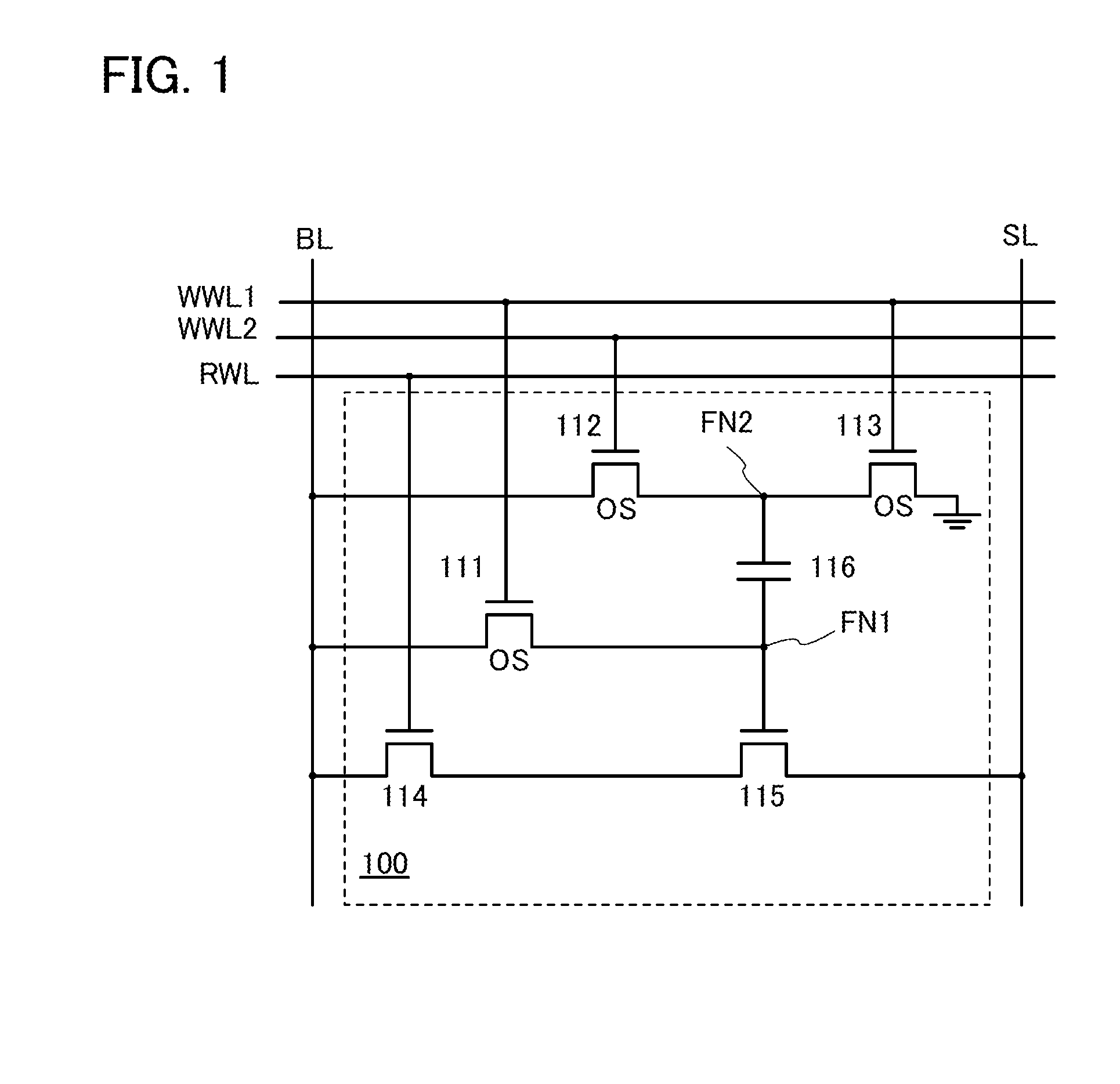
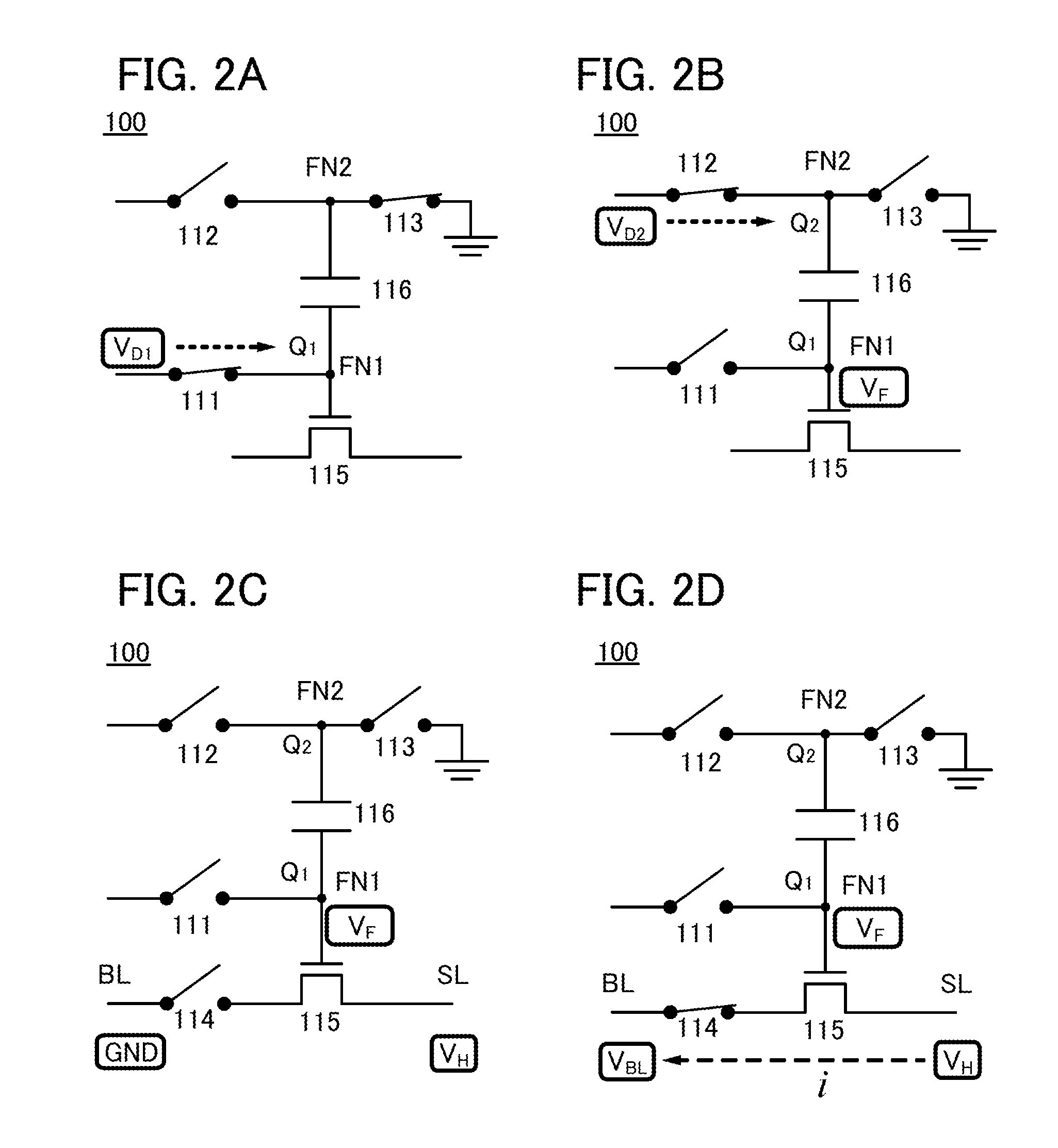
[0072]In this embodiment, a circuit configuration and operation of a memory cell included in a semiconductor device of one embodiment of the present invention will be described with reference to FIG. 1, FIGS. 2A to 2D, and FIGS. 3 to 6.

[0073]FIG. 1 is a circuit diagram of a memory cell 100 of one embodiment of the present invention.

[0074]The memory cell 100 illustrated in FIG. 1 includes a transistor 111, a transistor 112, a transistor 113, a transistor 114, a transistor 115, a capacitor 116, a node FN1, and a node FN2. Although not shown in FIG. 1, a plurality of memory cells 100 are actually arranged in a matrix.

[0075]A gate of the transistor 111 is connected to a write word line WWL1. One of a source and a drain of the transistor 111 is connected to a bit line BL. The other of the source and the drain of the transistor 111 is connected to the node FN1.

[0076]A gate of the transistor 112 is connected to a write word line WWL2. One of a source and a drain of the transistor 112 is co...

embodiment 2

[0154]In this embodiment, a circuit configuration and operation of a memory cell included in a semiconductor device of one embodiment of the present invention will be described with reference to FIG. 7, FIGS. 8A to 8D, and FIGS. 9 to 11.

[0155]FIG. 7 is a circuit diagram of a memory cell 101 of one embodiment of the present invention.

[0156]The memory cell 101 illustrated in FIG. 7 includes the transistor 111, the transistor 112, the transistor 113, the transistor 115, the capacitor 116, a capacitor 117, the node FN1, and the node FN2. Although not shown in FIG. 7, a plurality of memory cells 101 are actually arranged in a matrix.

[0157]The gate of the transistor 111 is connected to the write word line WWL1. One of the source and the drain of the transistor 111 is connected to the bit line BL. The other of the source and the drain of the transistor 111 is connected to the node FN1.

[0158]The gate of the transistor 112 is connected to the write word line WWL2. One of the source and the d...

embodiment 3

[0224]In this embodiment, an oxide semiconductor transistor that can be used as the transistors 111 to 113 shown in the foregoing embodiments will be described. Although the transistor 111 is given as an example below, the same description can apply to the transistors 112 and 113.

[0225]FIGS. 12A to 12D are a top view and cross-sectional views illustrating the transistor 111. FIG. 12A is the top view. FIG. 12B illustrates a cross section along the dashed-dotted line Y1-Y2 in FIG. 12A. FIG. 12C illustrates a cross section along the dashed-dotted line X1-X2 in FIG. 12A. FIG. 12D illustrates a cross section along the dashed-dotted line X3-X4 in FIG. 12A. In FIGS. 12A to 12D, some components are scaled up or down or omitted for easy understanding. In some cases, the direction of the dashed-dotted line Y1-Y2 is referred to as a channel length direction and the direction of the dashed-dotted line X1-X2 is referred to as a channel width direction.

[0226]Note that the channel length refers to...


PUM


Abstract

A novel semiconductor device where multilevel data can be written and read. The semiconductor device includes first to fifth transistors, a capacitor, a bit line, and a power supply line. Write operation is performed in such a manner that first data is supplied to a gate of the fifth transistor through the first transistor; the first transistor is turned off; second data is supplied to a second electrode of the capacitor through the second transistor to convert the first data into third data; and the second electrode of the capacitor are made electrically floating. The second electrode of the capacitor is initialized to GND through the third transistor. Read operation is performed by charging or discharging the bit line through the fourth transistor and the fifth transistor. The first to third transistors are preferably oxide semiconductor transistors.

Description

BACKGROUND OF THE INVENTION[0001]1. Field of the Invention[0002]The present invention relates to an object, a method, or a manufacturing method. In addition, the present invention relates to a process, a machine, manufacture, or a composition of matter. One embodiment of the present invention relates to a semiconductor device, a display device, a light-emitting device, a power storage device, a memory device, or a driving method thereof. In particular, one embodiment of the present invention relates to a semiconductor device, a display device, or a light-emitting device each including an oxide semiconductor.[0003]In this specification and the like, a semiconductor device generally refers to a device that can function by utilizing semiconductor characteristics. A display device, an electro-optical device, a semiconductor circuit, and an electronic device include a semiconductor device in some cases.[0004]2. Description of the Related Art[0005]Much attention has been focused on a semi...

Claims


Application Information

Patent Timeline
Patent Type & Authority Applications(United States)
IPC IPC(8): H01L27/108G11C7/12G11C5/14G11C11/419
CPCH01L27/10802H01L27/10897G11C5/14G11C7/12G11C11/419H01L27/0688G11C8/16G11C11/405G11C11/4087G11C2207/108G11C11/565H01L27/1225H10B12/315H10B12/33H10B12/36H10B12/036H10B12/056H10B12/50H10B12/0335H10B41/70H10B12/05H10B99/00H01L29/786G11C8/08G11C8/10G11C11/24G11C11/409H01L23/528H01L27/1207H01L27/1255H01L27/1259H01L29/24H01L29/7869
Inventor YAMAMOTO, YOSHITAKAKATO, KIYOSHI
Owner SEMICON ENERGY LAB CO LTD
Why Eureka
Try Eureka