Optical device

Active Publication Date: 2015-07-02
SEIKO EPSON CORP
View PDF2 Cites 43 Cited by
  • Summary
  • Abstract
  • Description
  • Claims
  • Application Information

AI Technical Summary

Benefits of technology

[0033]With this configuration, it is possible to use the above-described optical device as an illumination device and cause light to be emitted from any location of the illumination device when viewed from above. Therefore, it is possible to cause light to be emitted from only a location at which illumination is required while turning off light from the other locations, and thus the power consumption of the illumination device can be suppressed. Furthermore, since

Problems solved by technology

However, there is a problem with the biological information acquisition device disclosed in JPA-2009-172263 in that it is difficult to capture a

Method used


Image

  • Optical device
  • Optical device
  • Optical device

Examples


Example

Embodiment 1

[0042]Overview of Optical Device

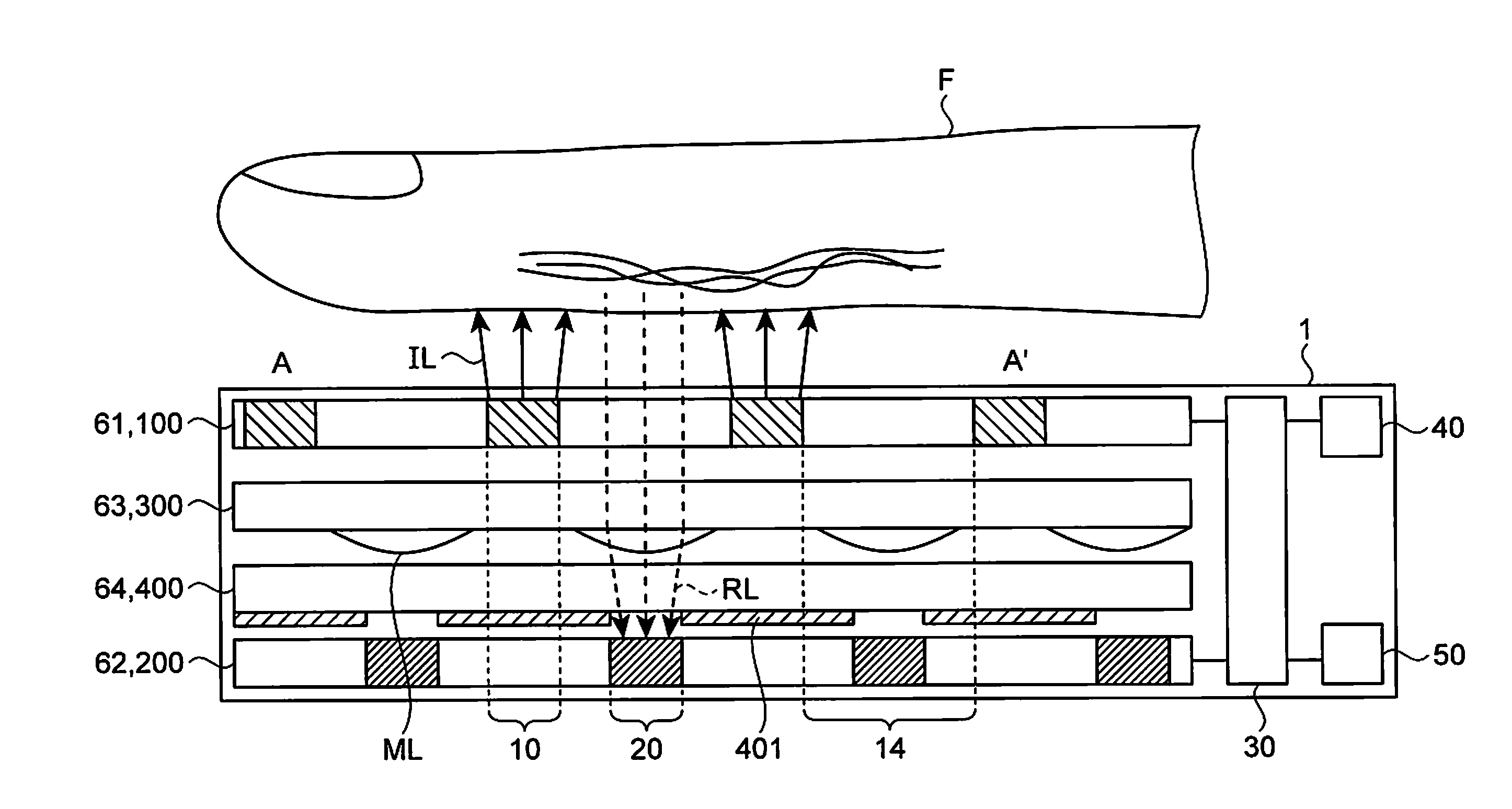
[0043]First, an overview of an optical device 1 will be described with reference to FIG. 1.

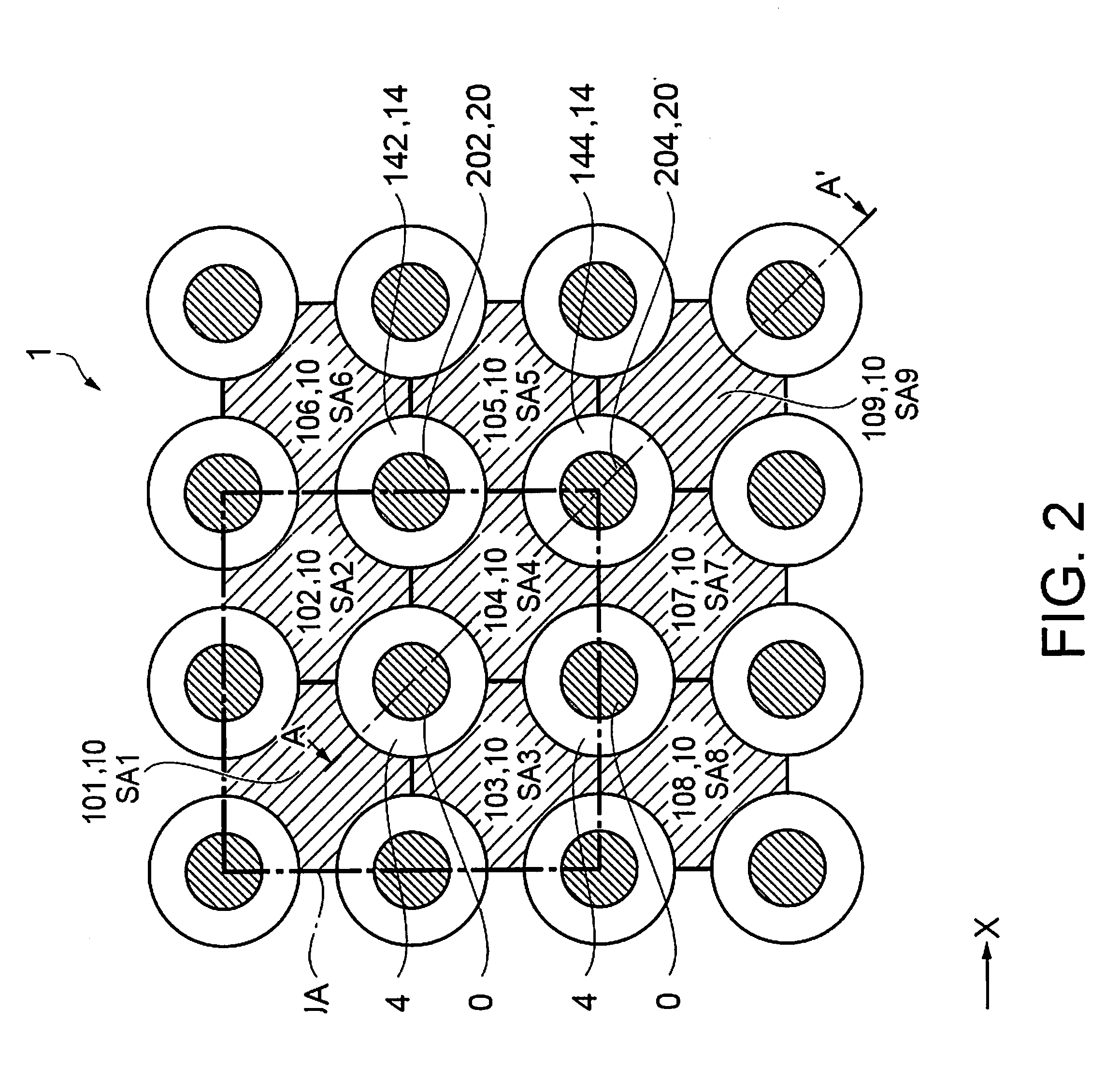
[0044]FIG. 1 is a cross-sectional view of an optical device according to this embodiment. In FIG. 1, a cross section taken along line A-A′ in a plan view shown in FIG. 2 is schematically shown by way of example. The optical device 1 includes light-emitting portions 10 and light-receiving portions 20, and irradiates a subject F such as the finger with irradiation light IL from the light-emitting portions 10 and receives reflected light RL from the subject F with the light-receiving portions 20. The light-emitting portions 10 and the light-receiving portions 20 are provided on the same side with respect to the subject F, and the light-emitting portions 10 are located closer to the subject F than the light-receiving portions 20 are. That is to say, the light-emitting portions 10 are located between the subject F such as the finger and the light-receivin...

Example

Embodiment 2

[0081]Form in which Illumination Device and Measurement Device are Formed in the Same Substrate

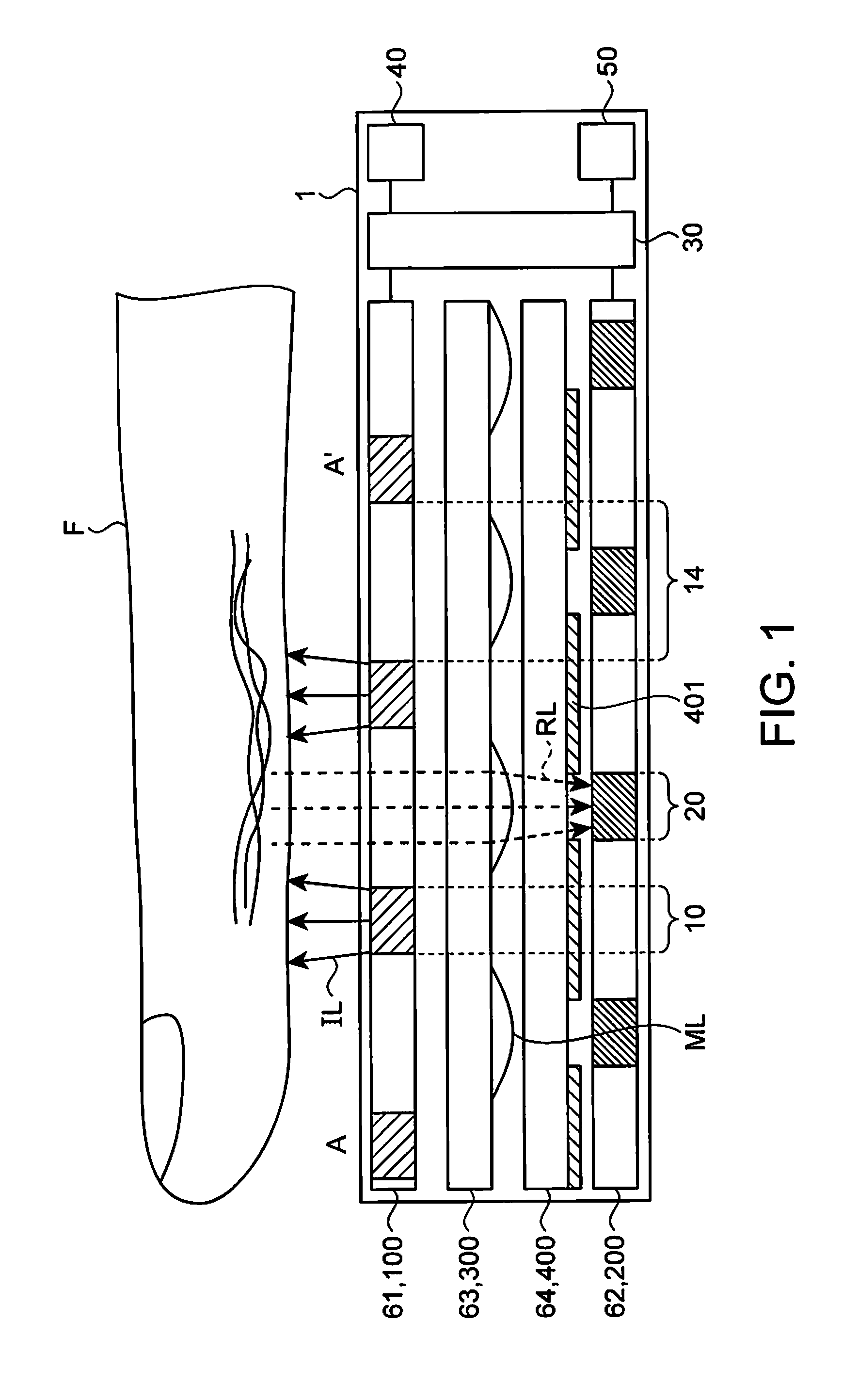
[0082]FIG. 5 is a cross-sectional view of an optical device according to this embodiment. In FIG. 5, by way of example, a cross section taken along line A-A′ in the plan view shown in FIG. 2 is schematically shown. Next, referring to FIG. 5, the optical device according to this embodiment will be described. It should be noted that the same components as those in Embodiment 1 are denoted by the same reference numerals, and redundant descriptions thereof are omitted. In Embodiment 1, the illumination device 100 is formed in the first substrate 61, and the measurement device 200 is formed in the second substrate 62. This embodiment differs from Embodiment 1 in that both the illumination device 100 and the measurement device 200 are formed in a fifth substrate 65. Otherwise, this embodiment is similar to Embodiment 1.

[0083]The control circuit is formed using thin film elements such...

Example

Embodiment 3

[0084]Form in which Control Circuit can be Recombined

[0085]Next, an optical device according to this embodiment will be described. It should be noted that the same components as those in Embodiments 1 and 2 are denoted by the same reference numerals, and redundant descriptions thereof are omitted. In Embodiment 1, the unit areas UA are fixed. This embodiment differs from Embodiment 1 in that the unit areas UA are variable.

[0086]In this embodiment, the control circuit can be recombined. Therefore, for example, in the case where light is to be received by the second light-receiving portion 202, a control circuit is constituted by the second control portion, the fourth control portion, the fifth control portion, and the sixth control portion, and the second light-emitting portion 102, the fourth light-emitting portion 104, the fifth light-emitting portion 105, and the sixth light-emitting portion 106 can be controlled by this control circuit so as to emit light. In this man...


PUM


Abstract

A high-performance optical device is provided. An optical device includes a first transmitting portion that is disposed at the center of a predetermined area in a first substrate, a light-receiving portion that receives light passing through the first transmitting portion, N light-emitting portions (N is an integer of 2 or more) that are disposed around the first transmitting portion in the predetermined area, and a control circuit that controls the light-emitting portions. The control circuit is functionally divided into N control portions, namely, first to N-th control portions. The N control portions are disposed in areas overlapping the N light-emitting portions, respectively, when viewed from above. The optical device can reduce noise light and achieve a high S/N ratio, and also the sensitivity of the optical device can be improved.

Description

[0001]This application claims the benefit of Japanese Patent Application No. 2013-270764, filed on Dec. 27, 2013. The content of the aforementioned application is incorporated herein by reference in its entirety.BACKGROUND[0002]1. Technical Field[0003]The present invention relates to the field of optical devices.[0004]2. Related Art[0005]In recent years, some biometric devices and image scanners have a light-emitting portion and a light-receiving portion that are disposed on the same side with respect to a subject (e.g., a part of a living body, an original, and the like) placed on a reading area and read an image of the subject by irradiating the subject with light from the light-emitting portion and receiving the reflected light with the light-receiving portion. For example, JP-A-2009-172263 discloses a biological information acquisition device that captures a vein image of the finger by irradiating the finger with light (near-infrared light) emitted from a light source using a pl...

Claims


Application Information

Patent Timeline
IPC IPC(8): H01L31/12H05B33/08H05B44/00
CPCH05B33/0896H01L31/125H01L27/14678H01L27/1462H01L27/14623H01L27/14627H01L27/14649G06V40/1324G06V40/14G06V40/1318G06V40/1365H10K59/65G06F1/00
Inventor YAMAMOTO, GAKUJI
Owner SEIKO EPSON CORP
Why Eureka
Try Eureka