Semiconductor light emitting device

a technology of light emitting devices and semiconductors, which is applied in the manufacture of semiconductor/solid-state devices, semiconductor devices, and semiconductor devices. it can solve the problems of insufficient brightness of insufficient expansion of the light transmitting area in such a practically enlarged appearance of the light emitting area, and insufficient light spreading to the edge portion of the light transmitting member. achieve the effect of convenient formation

Active Publication Date: 2015-07-02
NICHIA CORP
View PDF6 Cites 81 Cited by
  • Summary
  • Abstract
  • Description
  • Claims
  • Application Information

AI Technical Summary

Benefits of technology

[0060]As the planar dimensions of the side surfaces 43 of the light transmissive member 40 increases, the amount of the blue light exiting from the side surfaces 43 increases, whereby the effect on the reduction of the yellow ring phenomenon increases. For this reason, the thicker light transmissive member 40 is more preferable. On the other hand, the thinner light transmissive member 40 is more preferable, because the height of the light emitting device can be accordingly lower. The thickness of the light transmissive member 40 is preferably 0.05 mm to 0.15 mm, and with such thickness, the light emitting device can be made thin while advantageous effects of improving the light extraction efficiency and reducing the yellow ring phenomenon can be obtained.
[0061]Next, with reference to FIG. 5, a manufacturing method of the light emitting device 12 according to the present embodiment will be described. The present embodiment is different from the first embodiment in that the light reflecting layer 51 is formed (step 3) before the light transmissive member 40 is placed (step 2).<Step 1. Mounting Light Emitting Element 60>
[0062]In the same way as step 1 of the first embodiment, the housing 32 is formed, and the light emitting element 60 is mounted.<Step 3. Forming Light Reflecting Layer 51>
[0063]In the same way as step 3 of the first embodiment, the light reflecting layer 51 can be formed of a resin material to which light reflective substance is added (light reflective resin). After light reflective substance is added to a liquid resin material before being cured, the liquid resin material is dropped in a gap between the side walls 31 of the housing 32 and the light emitting element 60. The dropped liquid resin material comes first in contact with the upper surface 30a of the substrate 30 and then climbs up, by surface tension, the inner surfaces 31b of the side walls 31 and the side surfaces 63 of the light emitting element 60, and covers the surfaces thereof. In this way, the light reflecting layer 51 having a cross-sectional shape as shown in FIG. 5 is easily formed. Finally, the liquid resin material is cured to form the light reflecting layer 51.<Step 2. Placing Light Transmissive Member 40>
[0064]The light transmissive member 40 which has a larger planar dimension than that of the upper surface 61 of the light emitting element 60 is prepared, and is placed on the upper surface 61 of the light emitting element 60. Adhesive may cover not only the boundary between the upper surface 61 of the light emitting element 60 and the lower surface 42 of the light transmissive member 40 but also the lower surface 4i b of the outer extended part 45 of the light transmissive member 40. Different from the first embodiment, the side surfaces 63 of the light emitting element 60 are already covered with the light reflecting layer 51; therefore, the side surfaces 63 of the light emitting element 60 are not covered with the adhesive. The adhesive is cured to form the light transmissive adhesive layer 70.<Step 4. Forming Phosphor-Containing Layer 52>
[0065]In the same way as step 4 of the first embodiment, the phosphor-containing layer 52 can be formed of a resin material to which the phosphor 81 is added (phosphor-containing resin). After the phosphor 81 is added to a liquid resin material before being cured, the liquid resin material is dropped on the upper surface 41 of the light transmissive member 40. The dropped liquid resin material spreads from the upper surface 41 of the light transmissive member 40 to the side surfaces 43 of the light transmissive member 40, the lower surface 45b of the outer extended part 45, and the upper surface of the light reflecting layer 51, and fills the recessed portion 33. Finally, the liquid resin material is cured to form the phosphor-containing layer 52. In this way, the light emitting device 12 according to the present embodiment is obtained.MODIFIED EXAMPLE

Problems solved by technology

However, in the light emitting devices such as described in JP 2012-4303 A and JP 2010-192629 A, the light transmissive members do not have sufficient brightness at the edge portions compared with the central portions which are directly above the respective light emitting elements.
Thus, satisfactory expansion in such a practically enlarged appearance of the light emitting areas may not be attained.
The inventors have found that due to the phosphor contained in the light transmissive member, the light does not sufficiently spread to the edge part of the light transmissive member.

Method used


Image

  • Semiconductor light emitting device
  • Semiconductor light emitting device
  • Semiconductor light emitting device

Examples


first embodiment

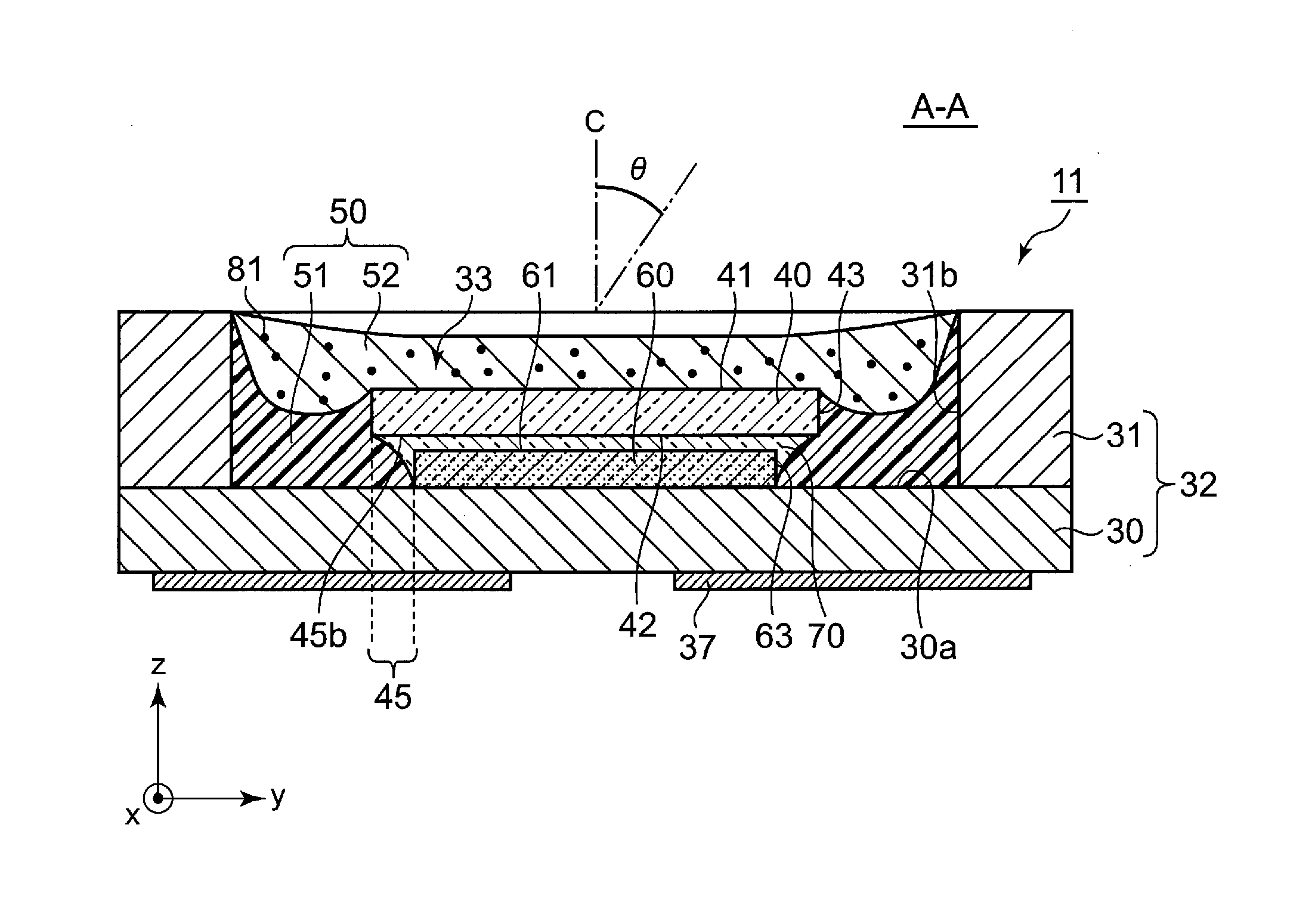
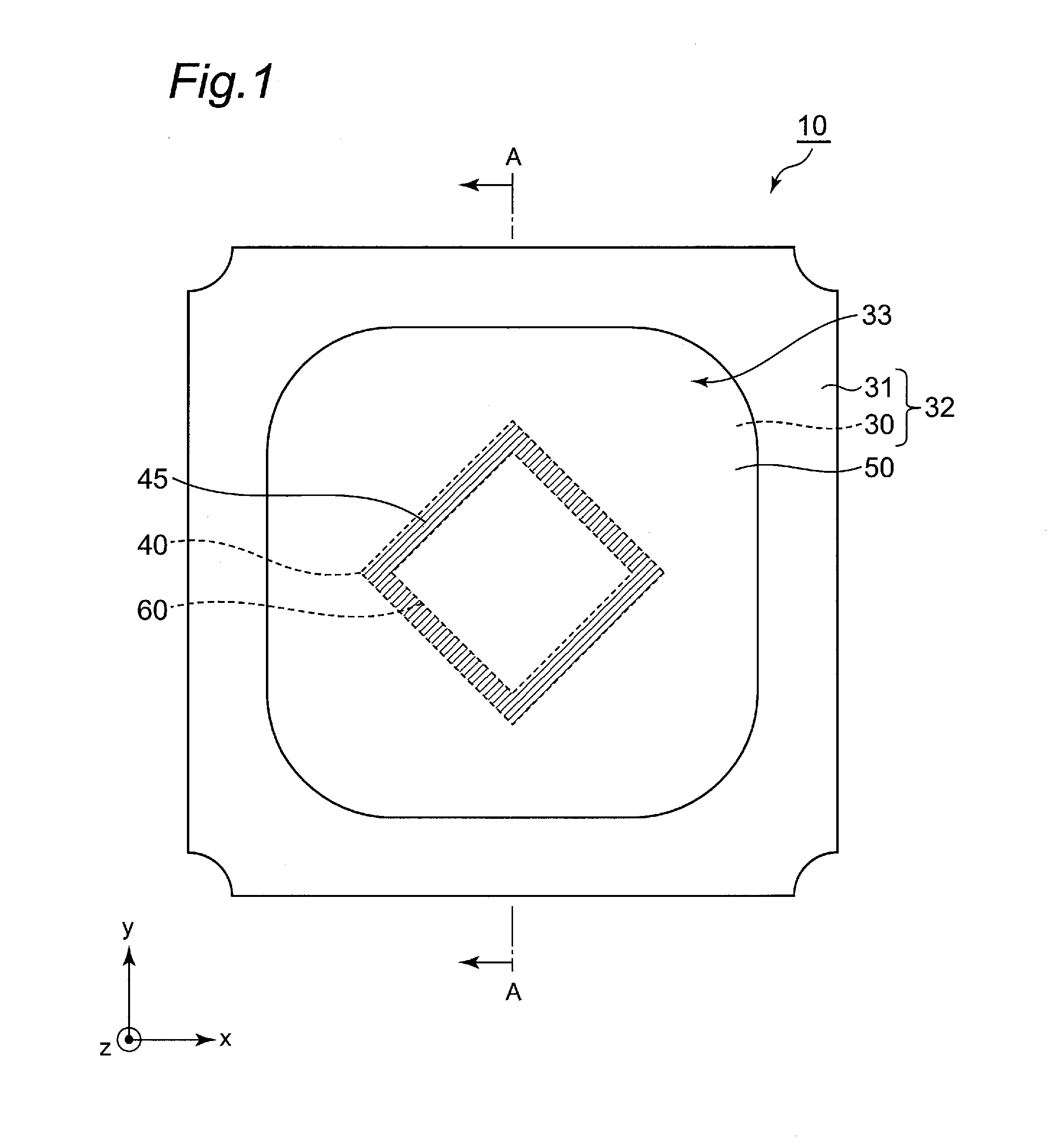
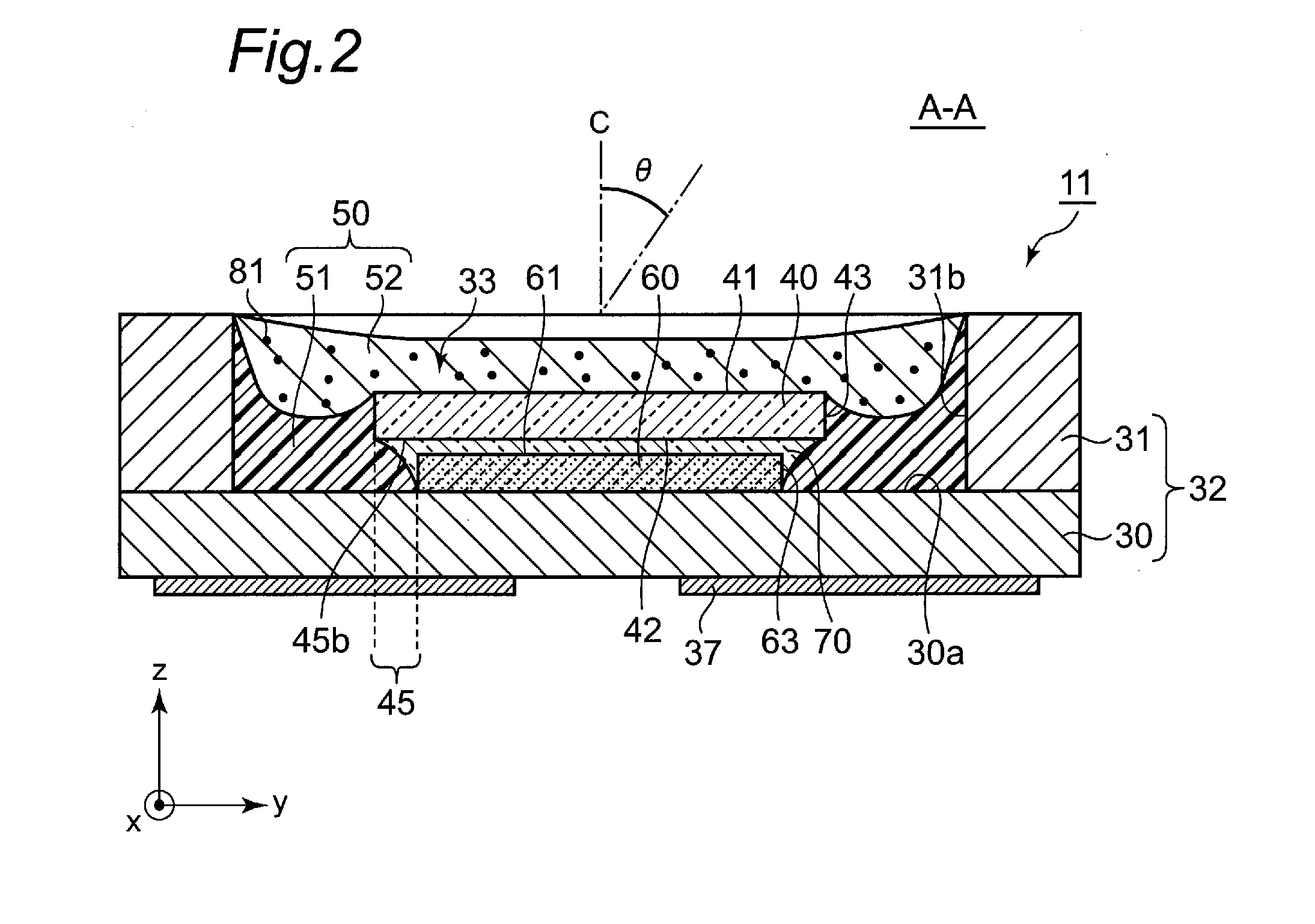
[0027]As shown in FIG. 1 and FIG. 2, a light emitting device 11 according to the present embodiment includes a housing 32 constituted of a substrate 30 and side walls 31, a light emitting element 60 mounted on an upper surface 30a of the substrate 30 in a recessed portion 33 of the housing 32, and a plate-shaped light transmissive member 40 placed over an upper surface 61 of the light emitting element 60. The light transmissive member 40 and the light emitting element 60 can be bonded by using, for example, pressure bonding, sintering, bonding with adhesive, or bonding with low melting point glass. In the light emitting device 11 according to the present embodiment, the light transmissive member 40 and the light emitting element are fixed with a light transmissive adhesive layer 70. The light emitting element 60 and the light transmissive member 40 in the recessed portion 33 are sealed with a sealing member 50 constituted of two layers. In the present embodiment, different from thos...

second embodiment

[0056]The light emitting device according to the present embodiment is largely different from the light emitting device 11 according to the first embodiment in that the sealing member 50 covering the side surfaces 43 of the light transmissive member 40 is changed from the light reflecting layer 51 to the phosphor-containing layer 52. In addition, the light emitting device according to the present embodiment is different from the light emitting device 11 according to the first embodiment also in that the side surfaces 63 of the light emitting element 60 is directly covered with the light reflecting layer 51. The other configuration is the same as that in the light emitting device 11 according to the first embodiment. Hereinafter, a description will be made on points in which the light emitting device according to the present embodiment is different from the light emitting device 11 according to the first embodiment.

[0057]As shown in FIG. 5, in a light emitting device 12 according to ...

modified example

[0066]FIG. 6 shows a light emitting device 12′ according to the modified example of the present embodiment. In the light emitting device 12′, in a phosphor-containing layer 52, a phosphor 81 is deposited on an upper surface 41 of a light transmissive member 40 and a boundary surface 55 between the phosphor-containing layer 52 and a light reflecting layer 51. However, the phosphor 81 is not deposited on the part under an outer extended part 45, and a phosphor layer 80 has a profile as shown in FIG. 6. Because the phosphor layer 80 does not substantially extend direct under the outer extended part 45, most of emitted light exiting downward from a lower surface 45b of the outer extended part 45 is reflected by the light reflecting layer 51 without colliding with the phosphor layer 80 (in other words, without being scattered by the phosphor 81 in the phosphor layer 80). Here, the upper surface (the boundary surface 55 ) of the light reflecting layer 51 has a cross-sectional shape of a s...


PUM

PropertyMeasurementUnit
thicknessaaaaaaaaaa
thicknessaaaaaaaaaa
lengthaaaaaaaaaa

Abstract

A light emitting device includes a substrate, a light emitting element mounted on the substrate, a light transmissive member placed on an upper surface of the light emitting element, and a sealing member which seals the light emitting element and the light transmissive member. The light transmissive member is a plate-shaped member not containing a phosphor and is larger than the light emitting element when viewed from above. The sealing member includes a first sealing member which is formed of a light reflecting member for reflecting light emitted from the light emitting element and covers side surfaces of the light emitting element, and a second sealing member which contains a phosphor for converting the light emitted from the light emitting element into light having wavelength different from wavelength of the light emitted from the light emitting element and covers at least an upper surface of the light transmissive member.

Description

CROSS-REFERENCE TO RELATED APPLICATION[0001]This application claims priority to Japanese Patent Application No. 2013-272592, filed on Dec. 27, 2013. The entire disclosure of Japanese Patent Application No. 2013-272592 is hereby incorporated herein by reference.BACKGROUND[0002]1. Field[0003]The present invention relates to semiconductor light emitting devices.[0004]2. Description of Related Art[0005]There have been known light emitting devices that include a light emitting element mounted on a mounting substrate, and a plate-shaped light transmissive member in which a phosphor is dispersed is disposed on an upper surface of the light emitting element (for example, JP 2012-4303 A and JP 2010-192629 A). In such light emitting devices, for example, a combination of a blue light emitting element as the light emitting element and a yellow phosphor which can wavelength-convert a blue light to a yellow light as the phosphor in the light transmissive member may be used. A part of the blue li...

Claims


Application Information

Patent Timeline
Patent Type & Authority Applications(United States)
IPC IPC(8): H01L33/50H01L33/48H01L33/60H01L33/54
CPCH01L33/507H01L33/54H01L33/486H01L2933/005H01L2933/0041H01L2933/0058H01L33/60H01L33/508H01L33/58H01L2924/181H01L33/56H01L2924/00012H01L25/0753H01L33/62H01L2933/0066
Inventor OZEKI, KENJIMIYOSHI, TOMONORI
Owner NICHIA CORP
Why Eureka
Try Eureka