Normally-off junction field-effect transistors and application to complementary circuits

Active Publication Date: 2015-07-23
IBM CORP
View PDF2 Cites 25 Cited by
  • Summary
  • Abstract
  • Description
  • Claims
  • Application Information

AI Technical Summary

Benefits of technology

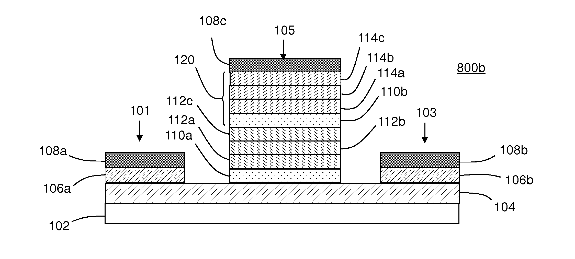
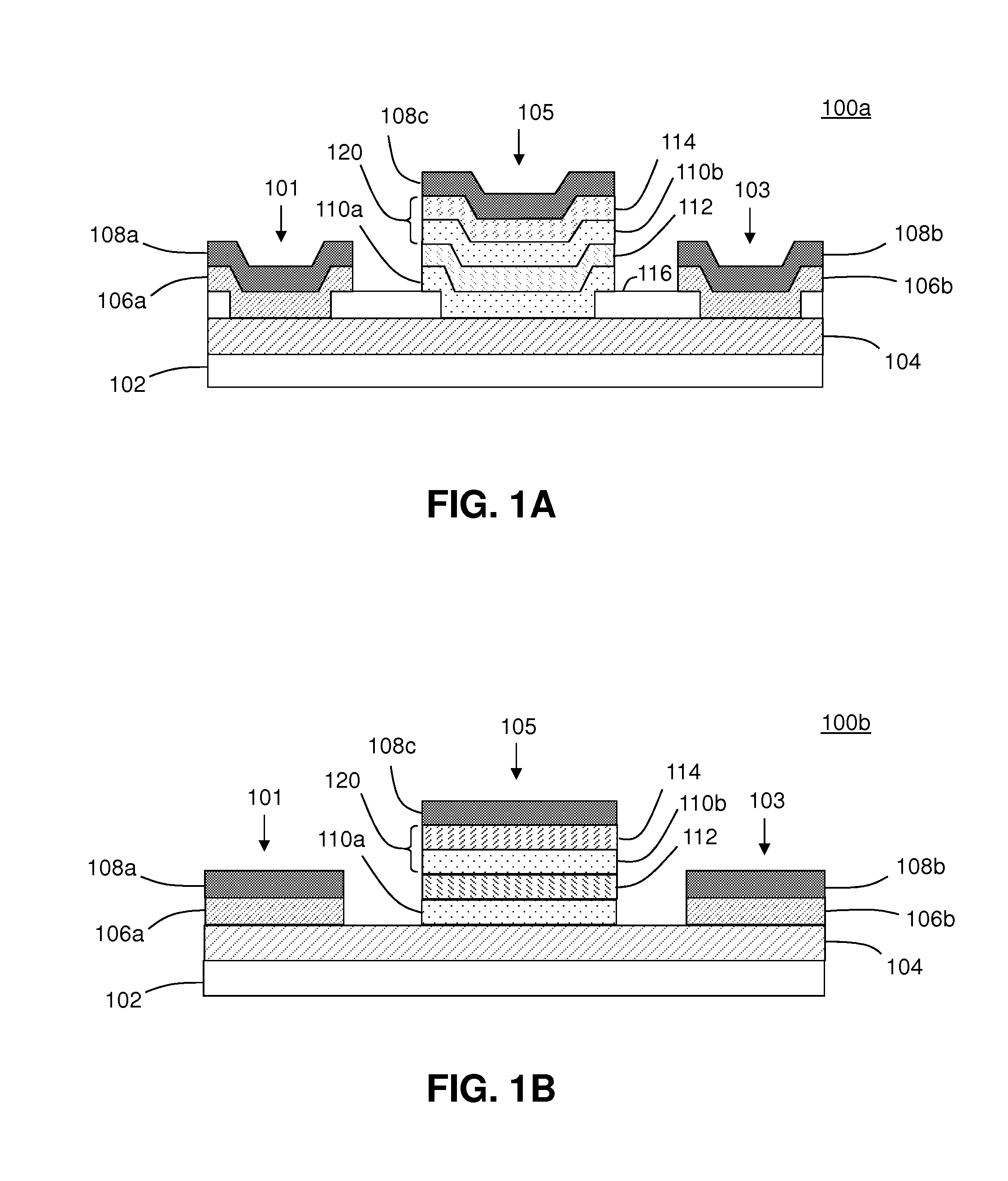
[0007]According to an aspect of the present invention, there is a junction field effect transistor (JFET) that includes a channel region and a gate region. The gate region includes a first gate sub-region and a second gate sub-region. The first gate sub-region forms a junction with the channel region. The second gate sub-region forms a junction with the first gate sub-region. The channel region and the second gate sub-region include material of a first conductivity type. The first gate sub-region includes material of a second conductivity type different from the first conductivity type.
[0008]According to another aspect of the present invention, there is a complementary circuit that includes a junction field effect transistor (JFET) and a metal-oxide-semiconductor field-effect transistor (MOSFET), each having a gate, drain, and source electrode and a channel region. The JFET includes a gate region. The gate region of the

Problems solved by technology

However, applications requiring large and stable drive currents such as high-resolution active-matrix organic light-emitting diode displays pose some challenges to the use of a-Si:H TFTs.
Large-area deposition techniques are typically suited for growing non-crystalline materials, but devices constructe

Method used


Image

  • Normally-off junction field-effect transistors and application to complementary circuits
  • Normally-off junction field-effect transistors and application to complementary circuits
  • Normally-off junction field-effect transistors and application to complementary circuits

Examples


Embodiment Construction

[0037]Some embodiments of the present invention recognize: (i) that thin-film heterojunction field-effect transistor (HJFET) devices with c-Si channels and PECVD contact regions (a) can be processed on thin single-crystalline substrates using the mainstream large area deposition techniques used for non-crystalline materials (for example, amorphous Si) and / or (b) provide substantially higher performance than a-Si:H TFTs; (ii) that the c-Si channel of such HJFET devices can be also formed by recrystallized polycrystalline silicon (poly-Si) using various known techniques; (iii) that the gate region of such an HJFET may be comprised of a-Si:H structurally similar to the emitter of heterojunction solar cells with intrinsic thin layers; (iv) that the source and drain regions may be comprised of hydrogenated crystalline silicon (c-Si:H) grown epitaxially on c-Si using the same PECVD reactor as a-Si:H at temperatures close to 200° C. (well below 250° C.); and / or (v) that this approach allow...


PUM


Abstract

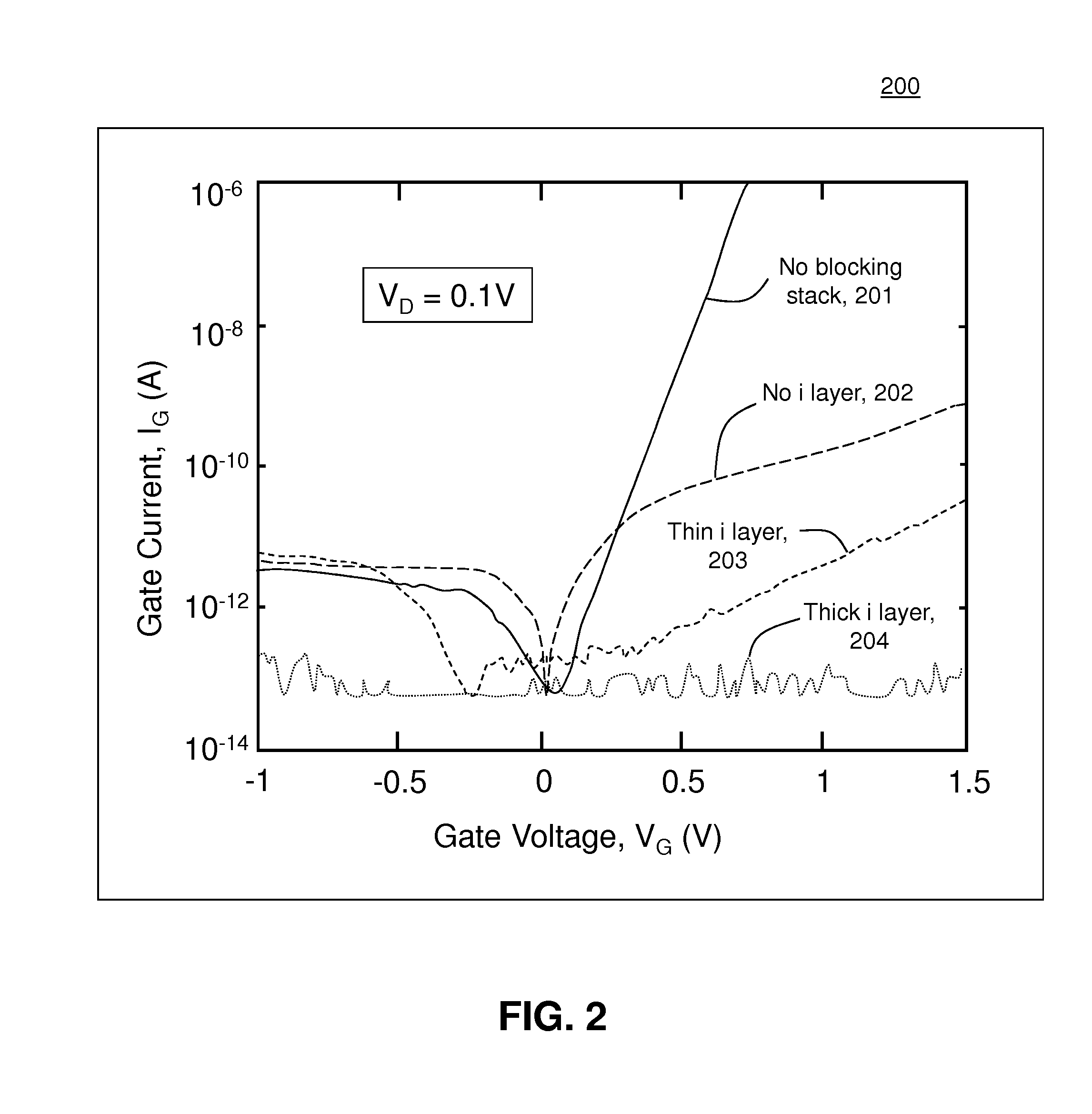
A junction field-effect transistor (JFET) with a gate region that includes two separate sub-regions having material of different conductivity types and/or a Schottky junction that substantially suppresses gate current when the gate junction is forward-biased, as well as complementary circuits that incorporate such JFET devices.

Description

STATEMENT ON PRIOR DISCLOSURES BY AN INVENTOR[0001]The following disclosure(s) are submitted under 35 U.S.C. 102(b)(1)(A) as prior disclosures by, or on behalf of, a sole inventor of the present application or a joint inventor of the present application:[0002](i) Hekmatshoar, Bahman, “Normally-Off Thin-Film Silicon Heterojunction Field-Effect Transistors and Application to Complementary Circuits,” IEEE Electron Device Letters, Vol. 35, No. 5, May 2014 (issue date), Mar. 14, 2014 (publication date).BACKGROUND OF THE INVENTION[0003]The present invention relates generally to the field of junction field-effect transistors (JFETs), and more particularly to structures for thin-film JFETs.[0004]Hydrogenated amorphous silicon (a-Si:H) enjoys widespread use in the production of thin-film transistors (TFTs), image sensors, photo-receptors and solar cells. This material is typically grown by plasma-enhanced chemical vapor deposition (PECVD) at temperatures close to 200° C., suitable for low-co...

Claims


Application Information

Patent Timeline
IPC IPC(8): H01L29/423H01L29/16H01L27/06H01L29/808H01L29/812
CPCH01L29/42312H01L29/8086H01L29/16H01L27/0617H01L29/812H01L27/098H01L29/1066H01L29/1604H01L29/8126H01L29/868H01L29/42316H01L29/802H01L29/8124
Inventor HEKMATSHOARTABARI, BAHMANSHAHIDI, GHAVAM G.
Owner IBM CORP
Why Eureka
Try Eureka