Normally-off junction field-effect transistors and application to complementary circuits

a junction field and transistor technology, applied in the direction of transistors, semiconductor devices, electrical equipment, etc., can solve the problems of inconvenient use of a-si:h tfts, device construction made from these materials suffers from inferior performance relative to those made from crystalline materials, and is too expensive for large-area electronics and displays

Active Publication Date: 2017-03-30
INT BUSINESS MASCH CORP
View PDF4 Cites 2 Cited by
  • Summary
  • Abstract
  • Description
  • Claims
  • Application Information

AI Technical Summary

Benefits of technology

The present invention describes a new structure for JFET and HJFET devices that includes an improved gate stack to block gate current at forward bias. These devices can also be used in the pixel circuits of active-matrix organic light-emitting diode (AMOLED) backplanes and can be manufactured using the same deposition techniques as mainstream large-area processing. Additionally, the invention also describes a method for forming complementary circuits through interconnection of the JFET and HJFET devices with MOSFET devices fabricated on the same substrate. These features make the new structure more efficient and better suited for use in high-density integrated circuits.

Problems solved by technology

However, applications requiring large and stable drive currents such as high-resolution active-matrix organic light-emitting diode displays pose some challenges to the use of a-Si:H TFTs.
Large-area deposition techniques are typically suited for growing non-crystalline materials, but devices constructed from these materials suffer from inferior performance relative to those made from crystalline materials.
At the same time, processing single-crystalline devices typically requires a complementary metal-oxide-semiconductor (CMOS) foundry, which is too expensive for large-area electronics and displays.

Method used


Image

  • Normally-off junction field-effect transistors and application to complementary circuits
  • Normally-off junction field-effect transistors and application to complementary circuits
  • Normally-off junction field-effect transistors and application to complementary circuits

Examples


Embodiment Construction

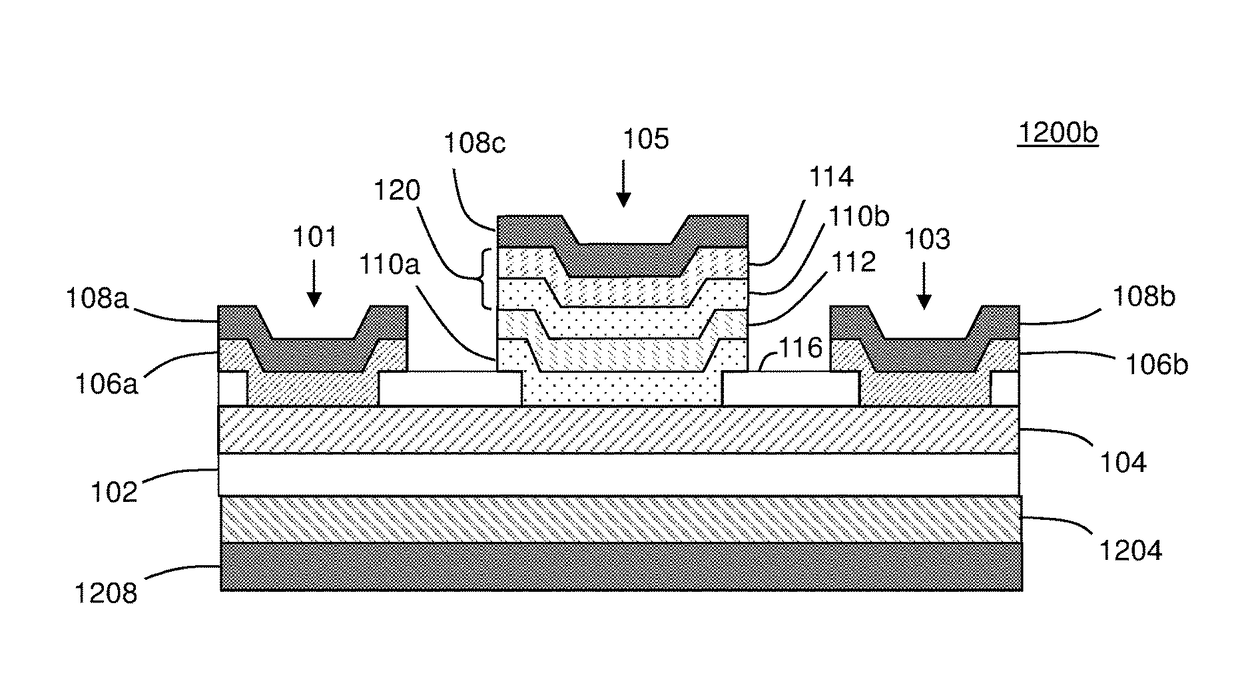
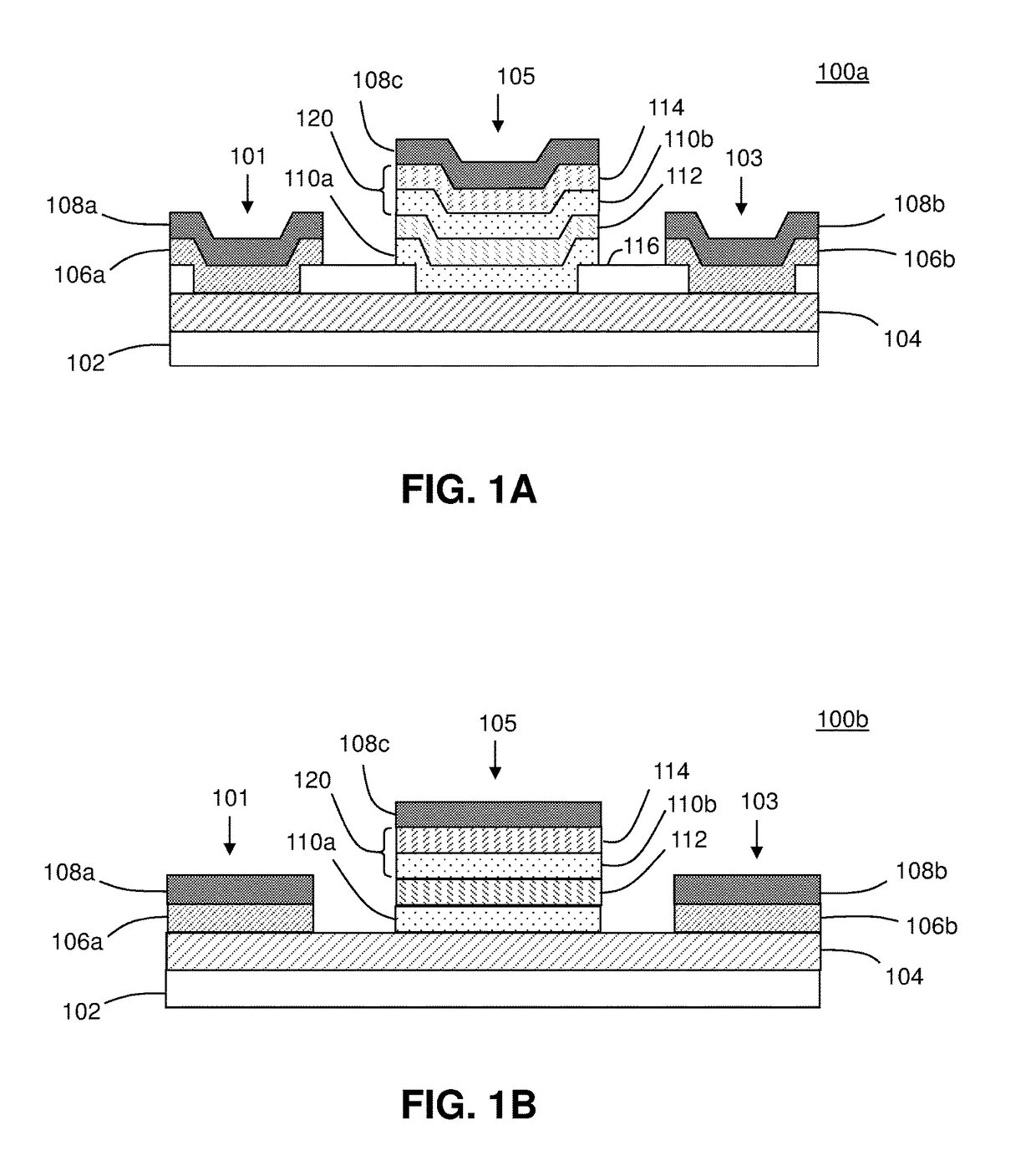
[0037]Some embodiments of the present invention recognize: (i) that thin-film heterojunction field-effect transistor (HJFET) devices with c-Si channels and PECVD contact regions (a) can be processed on thin single-crystalline substrates using the mainstream large area deposition techniques used for non-crystalline materials (for example, amorphous Si) and / or (b) provide substantially higher performance than a-Si:H TFTs; (ii) that the c-Si channel of such HJFET devices can be also formed by recrystallized polycrystalline silicon (poly-Si) using various known techniques; (iii) that the gate region of such an HJFET may be comprised of a-Si:H structurally similar to the emitter of heterojunction solar cells with intrinsic thin layers; (iv) that the source and drain regions may be comprised of hydrogenated crystalline silicon (c-Si:H) grown epitaxially on c-Si using the same PECVD reactor as a-Si:H at temperatures close to 200° C. (well below 250° C.); and / or (v) that this approach allow...


PUM

PropertyMeasurementUnit
currentaaaaaaaaaa

Abstract

A junction field-effect transistor (JFET) with a gate region that includes two separate sub-regions having material of different conductivity types and / or a Schottky junction that substantially suppresses gate current when the gate junction is forward-biased, as well as complementary circuits that incorporate such JFET devices.

Description

STATEMENT ON PRIOR DISCLOSURES BY AN INVENTOR[0001]The following disclosure(s) are submitted under 35 U.S.C. §102(b)(1)(A) as prior disclosures by, or on behalf of, a sole inventor of the present application or a joint inventor of the present application:[0002](i) Hekmatshoar, Bahman, “Normally-Off Thin-Film Silicon Heterojunction Field-Effect Transistors and Application to Complementary Circuits,” IEEE Electron Device Letters, Vol. 35, No. 5, May 2014 (issue date), Mar. 14, 2014 (publication date).BACKGROUND OF THE INVENTION[0003]The present invention relates generally to the field of junction field-effect transistors (JFETs), and more particularly to structures for thin-film JFETs.[0004]Hydrogenated amorphous silicon (a-Si:H) enjoys widespread use in the production of thin-film transistors (TFTs), image sensors, photo-receptors and solar cells. This material is typically grown by plasma-enhanced chemical vapor deposition (PECVD) at temperatures close to 200° C., suitable for low-c...

Claims


Application Information

Patent Timeline
Patent Type & Authority Applications(United States)
IPC IPC(8): H01L29/808H01L29/16H01L29/10H01L29/812H01L29/80
CPCH01L29/8086H01L29/8124H01L29/1604H01L29/1066H01L29/802H01L27/0617H01L27/098H01L29/8126H01L29/868H01L29/42316
Inventor HEKMATSHOARTABARI, BAHMANSHAHIDI, GHAVAM G.
Owner INT BUSINESS MASCH CORP
Why Eureka
Try Eureka