Chip assembling on adhesion layer or dielectric layer, extending beyond chip, on substrate

a technology of dielectric layer and adhesion layer, applied in the field of electronic modules, can solve the problems of high temperature and negatively affect the electronic chips, and achieve the effect of robustness and easy manufacturing

Inactive Publication Date: 2015-08-06
INFINEON TECH AG
View PDF9 Cites 4 Cited by
  • Summary
  • Abstract
  • Description
  • Claims
  • Application Information

AI Technical Summary

Benefits of technology

[0006]There might be a need for an electronic module which can be manufactured easily and be robust against errors.

Problems solved by technology

In conventional processes of the type described, high temperatures can occur, which may negatively affect the electronic chips.
Even a tilt-free mounting of electronic chips between two metallic substrates is a technological challenge.

Method used


Image

  • Chip assembling on adhesion layer or dielectric layer, extending beyond chip, on substrate
  • Chip assembling on adhesion layer or dielectric layer, extending beyond chip, on substrate
  • Chip assembling on adhesion layer or dielectric layer, extending beyond chip, on substrate

Examples


Embodiment Construction

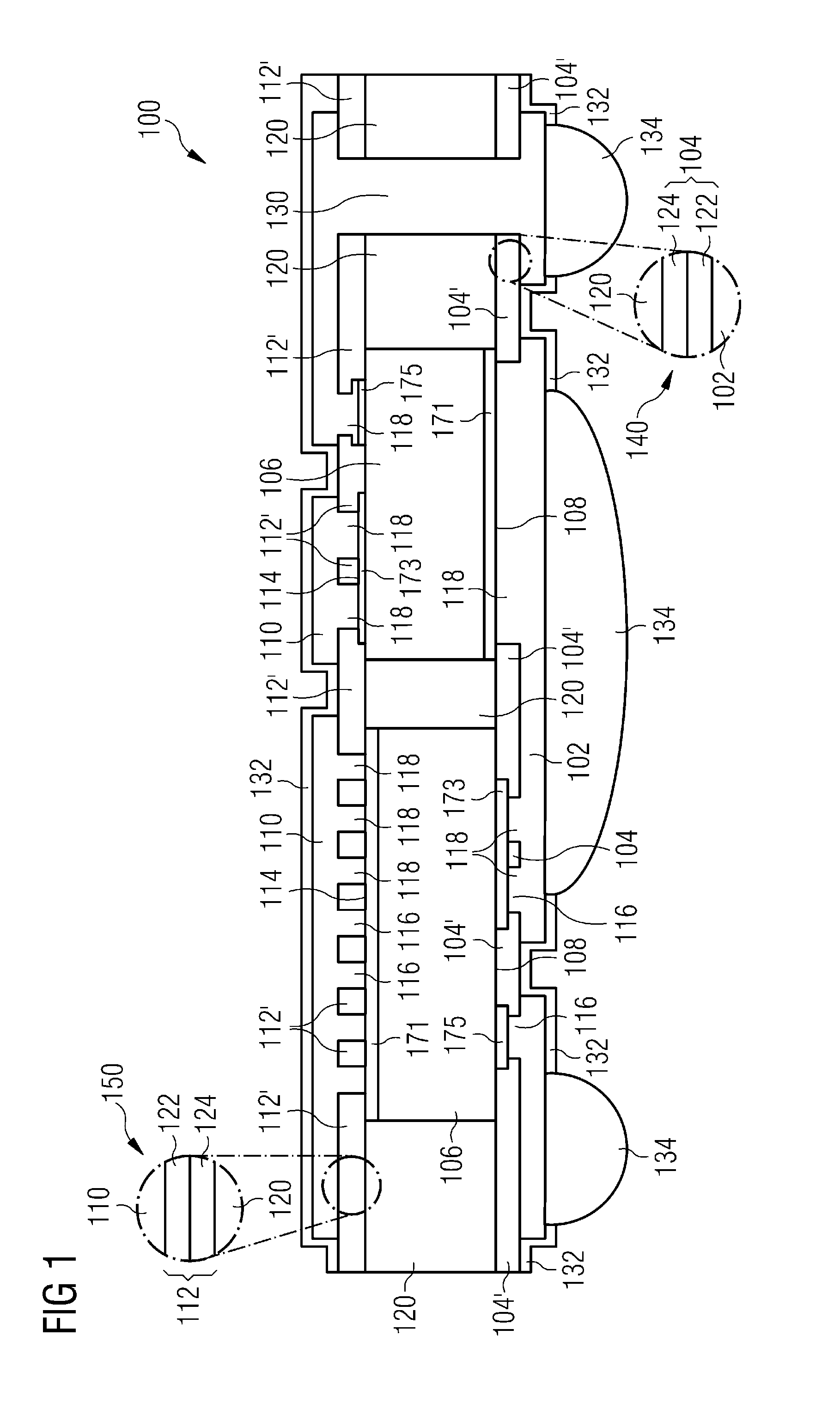
[0012]In the context of the present invention, the term “adhesion layer” can indicate in particular an extended and continuous layer with an even thickness of an adhesive material. The adhesive material can be so designed, that if an electronic chip (or other module component) is merely placed on the adhesive material, a mounting connection between the electronic chip (or the other module component) and the adhesion layer will be formed. In particular polymer, for example epoxy or filled epoxy, can be used as adhesion material of the adhesion layer.

[0013]In the context of the present invention, the term “dielectric layer” can describe in particular a layer composed of electrically insulating material that has been manufactured from the adhesion layer and forms part of the completed electronic module. Through a hardening of at least a part of the adhesion layer during manufacturing process, it can lose its adhesive nature entirely or partially and will therefore be indicated in the c...


PUM


Abstract

Electronic module (100), which comprises a first substrate (102), a first dielectric layer (104) on the first substrate (102), at least one electronic chip (106), which is mounted with a first main surface (108) directly or indirectly on partial region of the first dielectric layer (104), a second substrate (110) over a second main surface (114) of the at least one electronic chip (106), and an electrical contacting (116) for the electric contact of the at least one electronic chip (106) through the first dielectric layer (104), wherein the first adhesion layer (104) on the first substrate (102) extends over an area, which exceeds the first main surface (108).

Description

BACKGROUND[0001]1. Field[0002]Various embodiments in general relate to an electronic module and method for producing of at least one electronic module.[0003]2. Description of the State of the Art[0004]Electronic modules can comprise one or more electronic chips which are for example encapsulated in an encapsulation structure and can be connected to an electronic periphery through electrically conductive contacts.[0005]It is also possible to produce an electronic module, while electronic chips are mounted between two metallic substrates and spaces are filled with prepreg material. In conventional processes of the type described, high temperatures can occur, which may negatively affect the electronic chips. Even a tilt-free mounting of electronic chips between two metallic substrates is a technological challenge.SUMMARY[0006]There might be a need for an electronic module which can be manufactured easily and be robust against errors.[0007]According to an exemplary embodiment, an electr...

Claims


Application Information

Patent Timeline
Patent Type & Authority Applications(United States)
IPC IPC(8): H01L23/055H01L23/48H01L23/00H01L21/78
CPCH01L23/48H01L24/83H01L21/58H01L2224/83005H01L21/561H01L21/568H01L23/5389H01L24/25H01L24/97H01L2224/04105H01L2224/2518H01L2224/73267H01L21/78H01L23/055H01L23/481H01L23/50H01L2924/13055H01L2924/12042H01L2924/13091H01L23/49816H01L23/5384H01L23/5385H01L2224/83132H01L2224/24137H01L2224/32225H01L2224/82039H01L2224/83191H01L2224/83192H01L2224/92144H01L2224/97H01L24/82H01L2224/0603H01L2224/06181H01L2924/00H01L2224/82H01L2224/83H01L21/4853H01L21/486H01L23/5386H01L2224/8285
Inventor PALM, PETTERISCHARF, THORSTENWOMBACHER, RALF
Owner INFINEON TECH AG
Why Eureka
Try Eureka