Optical sensor device

a sensor device and optical sensor technology, applied in the direction of optical radiation measurement, semiconductor/solid-state device details, instruments, etc., can solve the problems of low adhesion of the surface of the metal to the resin, low force of the lead, and prone to cracking and peeling of the resin, etc., to achieve high adhesion, less prone to stress, and high air tightness

Inactive Publication Date: 2015-08-06
SII SEMICONDUCTOR CORP
View PDF2 Cites 8 Cited by
  • Summary
  • Abstract
  • Description
  • Claims
  • Application Information

AI Technical Summary

Benefits of technology

[0016]The optical sensor device according to one embodiment of the present invention can have a hollow structure in which the optical sensor element is sealed. In addition, the peripheries of the lead having the wire bonding portion exposed and the die pad are subjected to contact fitting molding with the first resin molded portion integrated by resin molding, and the periphery of the first resin molded portion, in which the wire bonding portion and the die pad surface are arranged on the bottomed portion, is subjected to contact fitting molding with the second resin molded portion so as to form the integrated package structure having the cavity. Thus, in a structure in which the periphery of the optical sensor element is molded with a resin, stress applied to the optical sensor element is removed. Moreover, the interface between the die pad and lead and the resin is allowed to have high adhesion and high airtightness, and contact fitting with a strong holding force of the lead can be achieved.
[0017]Further, the lead is bent and cut so as to also serve as the external lead terminal. The first resin molded portion and the second resin molded portion hold the lead. Therefore, at least mechanical stress applied to the lead can be received and alleviated by the second resin molded portion. In addition, the lead held even by the first resin molded portion is less liable to receive stress, and water and the like can be prevented from entering the package. Therefore, even in a package having a risk in that the factor for degrading reliability may be increased due to the increase in number of lead terminals, based on the fact that the mechanical stress and the entrance path of the water and the like increase in proportional to the number of the external lead terminals, an optical sensor device excellent in stability of characteristics and reliability can be provided.

Problems solved by technology

In this structure, there are the following problems: the removal preventing force of the lead is low; the holding area thereof is small; and the lead surface made of a metal has low adhesion to the resin.
Further, in the case where the part of the lead 25 serving as the external lead terminal is bent and cut, mechanical stress is concentrated on a root portion between the molding resin and the lead 25 exposed to outside from the molding resin, so that the resin is liable to be peeled and cracked.
Further, a gap remains at an interface between the lead 25 and the resin, with the result that the package has low airtightness.
Therefore, it is difficult to obtain a strong holding force of the lead 25.
Further, there is also a problem in that water is liable to enter the package from outside, and in addition, ambient environment may change.
Thus, it becomes more difficult to obtain high reliability.
However, even in the structure in which the periphery of the lead 25 is sealed with the transparent mold resin 28 formed of an epoxy resin, the adhesion between the metal and the resin is not sufficient, and there is a significant difference in expansion coefficient between the metal and the resin.
In addition, there is a risk in that an external appearance of the package may be impaired.

Method used


Image

  • Optical sensor device
  • Optical sensor device
  • Optical sensor device

Examples


first embodiment

[0038]Now, a configuration of an optical sensor device according to a first embodiment of the present invention is described with reference to the drawings.

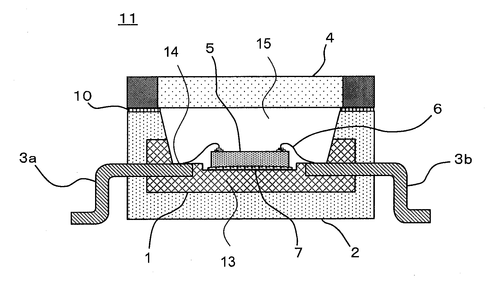
[0039]FIG. 1 is a schematic vertical sectional view of an optical sensor device 11 according to this embodiment. A resin molded portion having a cavity 15 is formed of a double molding structure in which a first resin molded portion 1 and a second resin molded portion 2 are subjected to contact fitting molding. The first resin molded portion 1 has a structure in which a part of leads 3a and 3b made of metals is subjected to contact fitting molding through use of a resin, and an element mounting portion 13 is integrally molded on a bottomed portion of the cavity 15. The peripheries of the leads 3a and 3b, excluding a wire bonding portion 14 and a portion exposed to outside through a package as an external lead terminal, are molded with the first resin molded portion 1. The periphery of the first resin molded portion 1 is subjected...

second embodiment

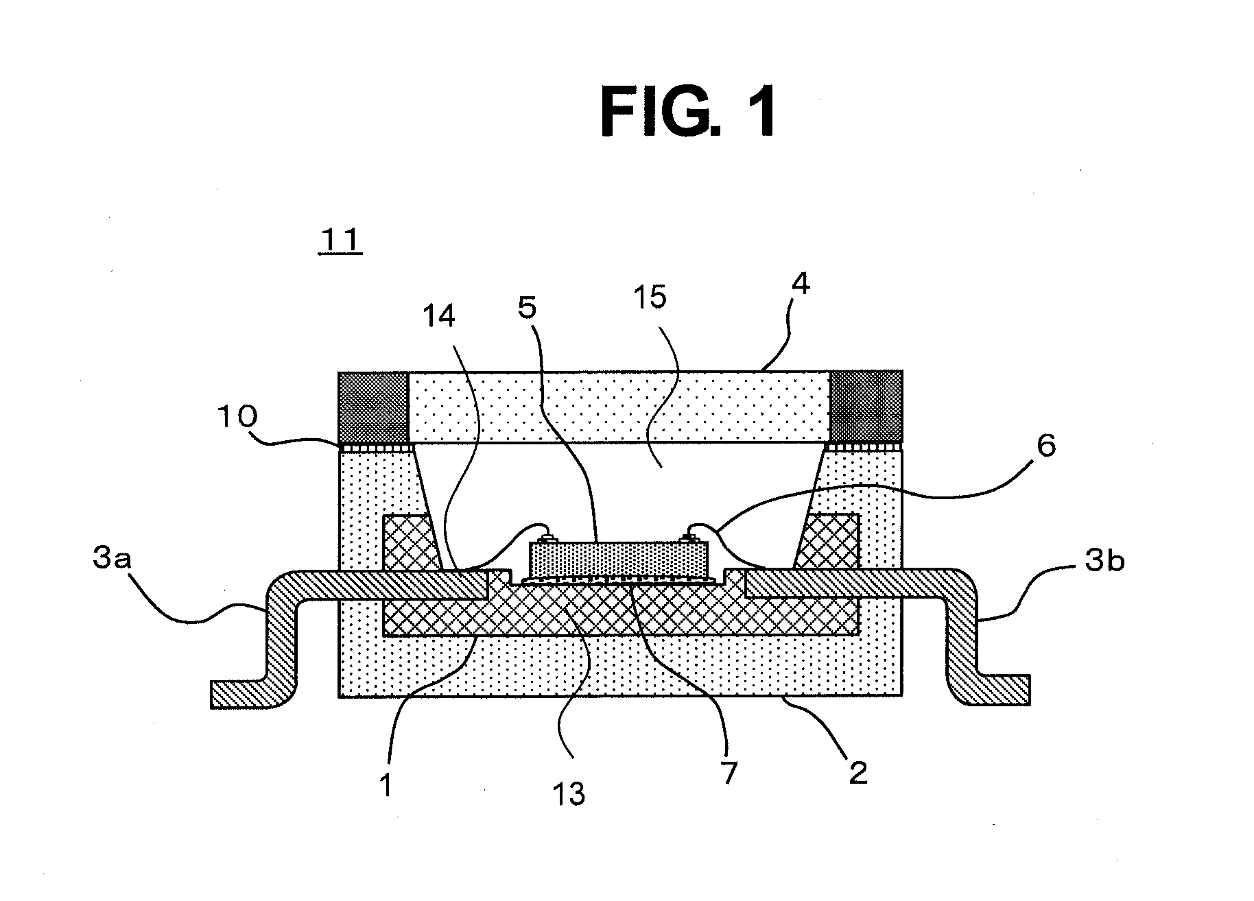
[0046]FIG. 2A is a sectional view of an optical sensor device 11 according to a second embodiment of the present invention. FIG. 2B is a front view of a first resin molded portion 1, and FIG. 2C is a sectional view thereof. FIG. 2A illustrates a cross section of a package body having a cavity, excluding a glass substrate 4 having a filter function, in the optical sensor device 11. The optical sensor device 11 has a structure in which a die pad portion 8 formed of a metal frame is provided on the first resin molded portion 1. The first resin molded portion 1 has a structure in which the periphery of the die pad portion 8 formed of a metal frame, excluding a surface side on which an optical sensor element 5 is to be mounted, and the periphery of each lead, excluding a portion in which a frame surface to be used as a wire bonding portion is exposed, are molded with a resin so as to be integrated.

[0047]Further, FIG. 2B illustrates a front view of the first resin molded portion 1 having ...

third embodiment

[0048]FIG. 3 is a sectional view of an optical sensor device 11 according to a third embodiment of the present invention. Ina first resin molded portion 1, a part of a die pad portion 8 formed of a metal frame on which an optical sensor element 5 is to be mounted is molded so as to increase thickness, and a bottom surface of the die pad portion 8 on which the optical sensor element 5 is to be mounted is exposed from a surface of a second resin molded portion 2 corresponding to a back surface of a package. The bottom surface of the die pad portion 8 is not covered with a resin forming the second resin forming portion 2. Thus, a double molding structure is achieved which has a heat dissipation function capable of releasing heat, generated from the mounted optical sensor element 5, to outside through an adhesive 7 via the die pad portion 8.


PUM


Abstract

A package for an optical sensor device has a double molding structure in which a first resin molded portion (1) and a second resin molded portion (2) are subjected to contact fitting. The first resin molded portion (1) has a structure in which peripheries of a die pad portion (8) on which an optical sensor element (5) is mounted and a part of leads (3a, 3b) are molded with a resin so as to be integrated. The second resin molded portion (2) has a structure in which the periphery of the first resin molded portion (1) is molded with a resin so as to form an outer shape. When a cavity is formed, a glass substrate (4) having a filter function and an upper surface of the resin molded portions are bonded to each other to form a cavity structure.

Description

BACKGROUND OF THE INVENTION[0001]1. Field of the Invention[0002]The present invention relates to an optical sensor device. More specifically, the present invention relates to a package structure of the optical sensor device.[0003]2. Description of the Related Art[0004]FIG. 11 is a sectional view illustrating an example of a related-art package (FIG. 2 of Japanese Patent Application Laid-open No. 2002-198455). This package has the following structure. A package body 21 includes a lead 25 and a cavity formed by a bottomed portion 23 and an inner side surface 24 that are made of a resin material. A semiconductor element 22 is mounted on the bottomed portion 23 of the package body 21, and a lid 27 is provided on a package upper surface. A surface of a part of the lead 25 is exposed from the bottomed portion 23, and another part of the lead 25 is exposed to outside through the package formed of a resin molded portion so as to be used as an external terminal. An electrode is formed on a s...

Claims


Application Information

Patent Timeline
Patent Type & Authority Applications(United States)
IPC IPC(8): H01L31/0203H01L31/02H01L31/0232
CPCH01L31/02002H01L31/02325H01L31/0203H01L2224/48091H01L2224/48247H01L2224/73265H01L2924/181H01L2924/00014H01L2924/00012G01J1/0271H01L27/14H01L23/3157H01L23/49838H01L31/02162
Inventor TSUKAGOSHI, KOJI
Owner SII SEMICONDUCTOR CORP
Why Eureka
Try Eureka