Electronic device
a technology of electronic devices and batteries, applied in the direction of electric apparatus casings/cabinets/drawers, liquid/fluent solid measurements, instruments, etc., can solve the problems of battery capacity reduction, battery size and thickness reduction, and large size and weight of electronic devices, so as to prolong the usage period of electronic devices and prolong the usage period
- Summary
- Abstract
- Description
- Claims
- Application Information
AI Technical Summary
Benefits of technology
Problems solved by technology
Method used
Image

Examples
embodiment 1
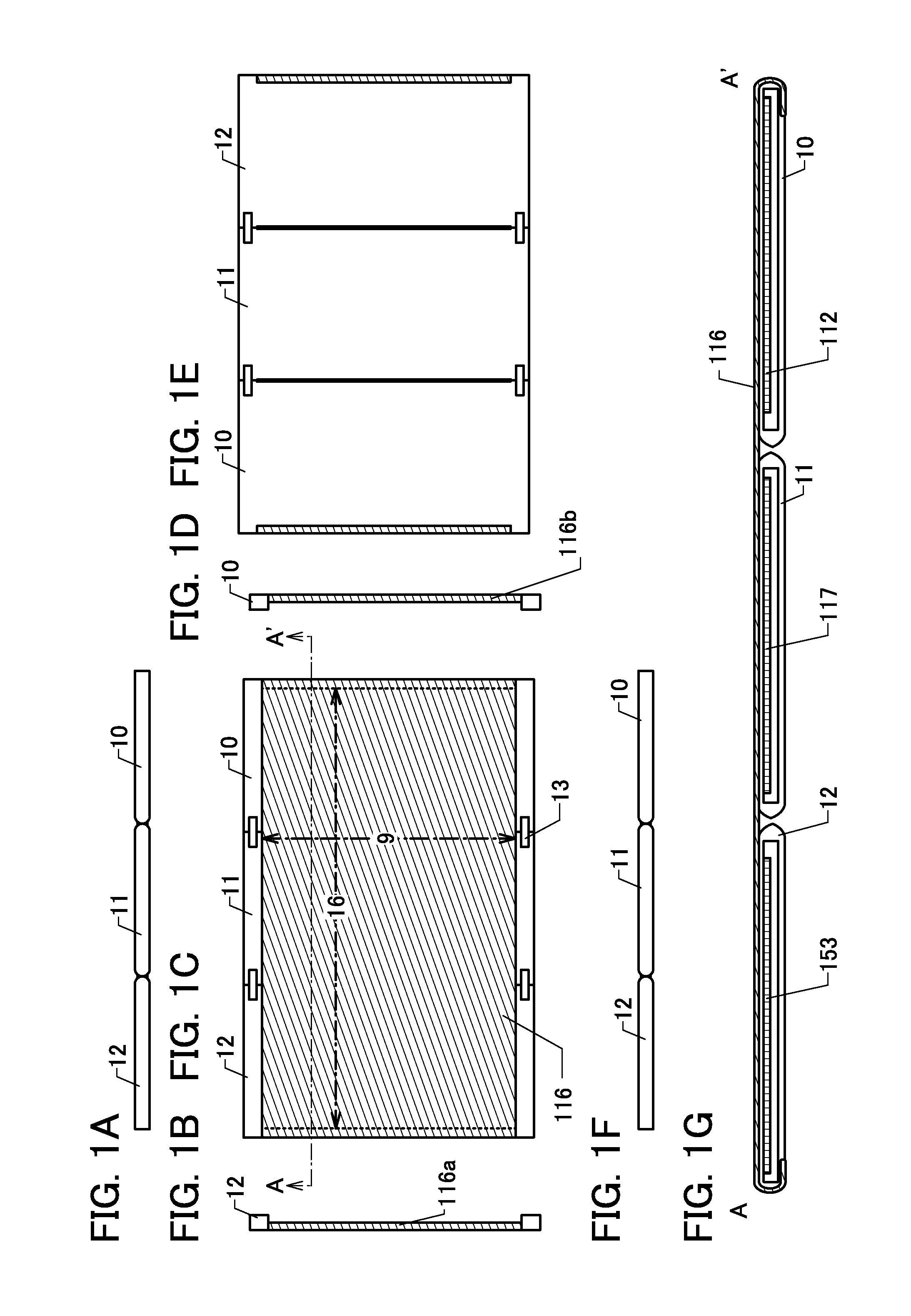
[0082]In this embodiment, examples of electronic devices each provided with a display portion including a plurality of bendable portions will be described as novel devices that are highly convenient or reliable with reference to FIGS. 1A to 1G, FIGS. 2A to 2C, FIGS. 3A to 3F, FIG. 4, FIGS. 5A to 5C, FIG. 6, FIGS. 17A to 17C, and FIGS. 18A to 18D. Components of the electronic devices will be described below. Note that these components cannot be clearly distinguished and one component also serves as another component or includes part of another component in some cases.
[0083]A user can manually select any of the following two modes for the electronic device of this embodiment: a mode of folding the device to make it small by bending the plurality of bendable portions of the display portion; and a mode of unfolding the display portion.
[0084]FIGS. 1A to 1G illustrate the unfolded electronic device. FIG. 1A is a top view. FIG. 1B is a left side view. FIG. 1C is a front view illustrating a...
embodiment 2
[0145]In this embodiment, an example that is partly different from Embodiment 1 will be described with reference to FIGS. 7A to 7C. Note that the same reference numerals are used for the same portions as those in FIGS. 2A to 2C, and description of the portions with the same reference numerals is omitted here.
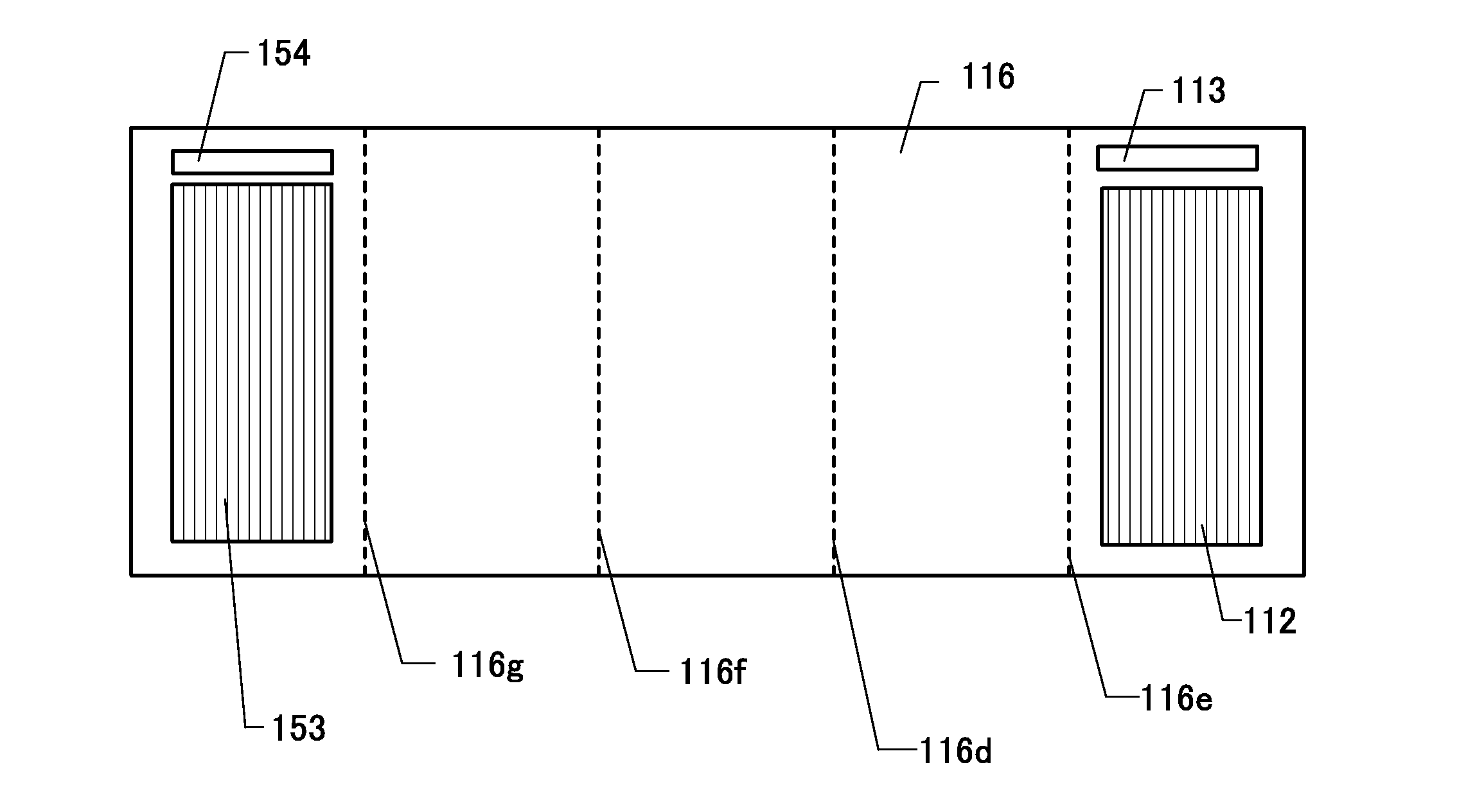
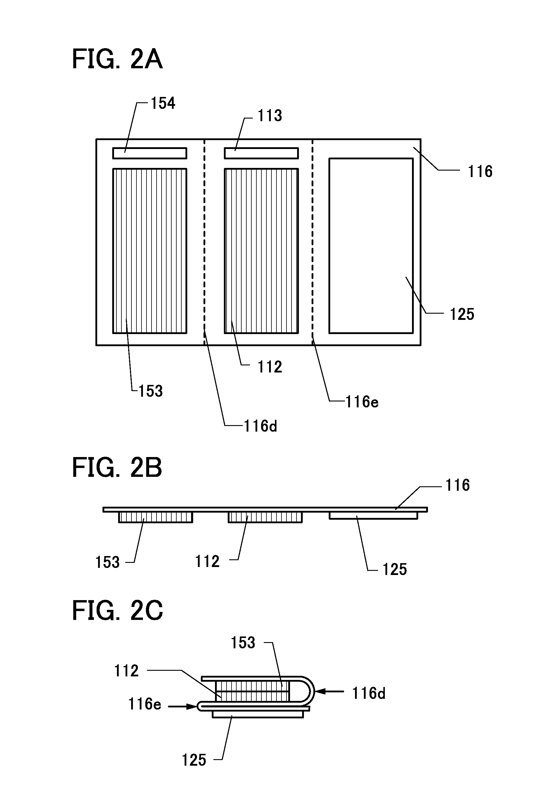
[0146]An example where two batteries with substantially the same size are used is described in Embodiment 1, whereas FIG. 7A illustrates an example where batteries have a different size and arrangement from the batteries in Embodiment 1. A display region of the display portion 116 has a size of approximately 5.9 inches.
[0147]FIG. 7A is a schematic view illustrating the arrangement of the batteries and the display portion 116 of the back surface, which is not a display surface. The bendable portion 116d of the display portion indicated by a dotted line in FIG. 7A is located between the battery 112 and a battery 753.
[0148]The battery 112 is electrically connected to the regulator ...
embodiment 3
[0160]In Embodiment 1, the display portion using the first flexible film 143 and the second flexible film 144 is described, whereas in this embodiment, a flexible display panel is fabricated using a separation method. In this embodiment, an example of fabricating the flexible display panel using a separation layer will be described below.
[0161]First, a separation layer 203 is formed over a formation substrate 201, and a layer 205 to be separated (hereinafter referred to as a layer 205) is formed over the separation layer 203 (FIG. 8A). In addition, a separation layer 223 is formed over a formation substrate 221, and a layer 225 to be separated (hereinafter referred to as a layer 225) is formed over the separation layer 223 (FIG. 8B).
[0162]For example, when a tungsten film is used as the separation layer, a tungsten oxide film can be formed between a layer to be separated and the tungsten film by N2O plasma treatment. Forming the tungsten oxide film by N2O plasma treatment enables se...
PUM
 Abstract
Description
Claims
Application Information
 - Generate Ideas
- Intellectual Property
- Life Sciences
- Materials
- Tech Scout
- Unparalleled Data Quality
- Higher Quality Content
- 60% Fewer Hallucinations
Browse by: Latest US Patents, China's latest patents, Technical Efficacy Thesaurus, Application Domain, Technology Topic, Popular Technical Reports.
© 2025 PatSnap. All rights reserved.Legal|Privacy policy|Modern Slavery Act Transparency Statement|Sitemap|About US| Contact US: help@patsnap.com