

Structure and the associated manufacturing process for a single-sided multi-layer mutual capacitance touch panel
a capacitance sensing and capacitance technology, applied in the field of electrical devices, can solve the problems of difficult use in producing thinner products, low product yield, and limited design, and achieve the effect of thin touch function structure, cost-effectiveness, and thin touch panel
- Summary
- Abstract
- Description
- Claims
- Application Information
AI Technical Summary
Benefits of technology
Problems solved by technology
Method used
Image

Examples
example
[0041]An example of manufacturing the capacitive touch function structure of the present subject matter is described and illustrated below. The present subject matter is capable of modifications in various obvious aspects, all without departing from the spirit and scope of the present subject matter. The drawings and detailed description are to be regarded as illustrative in nature and not restrictive.
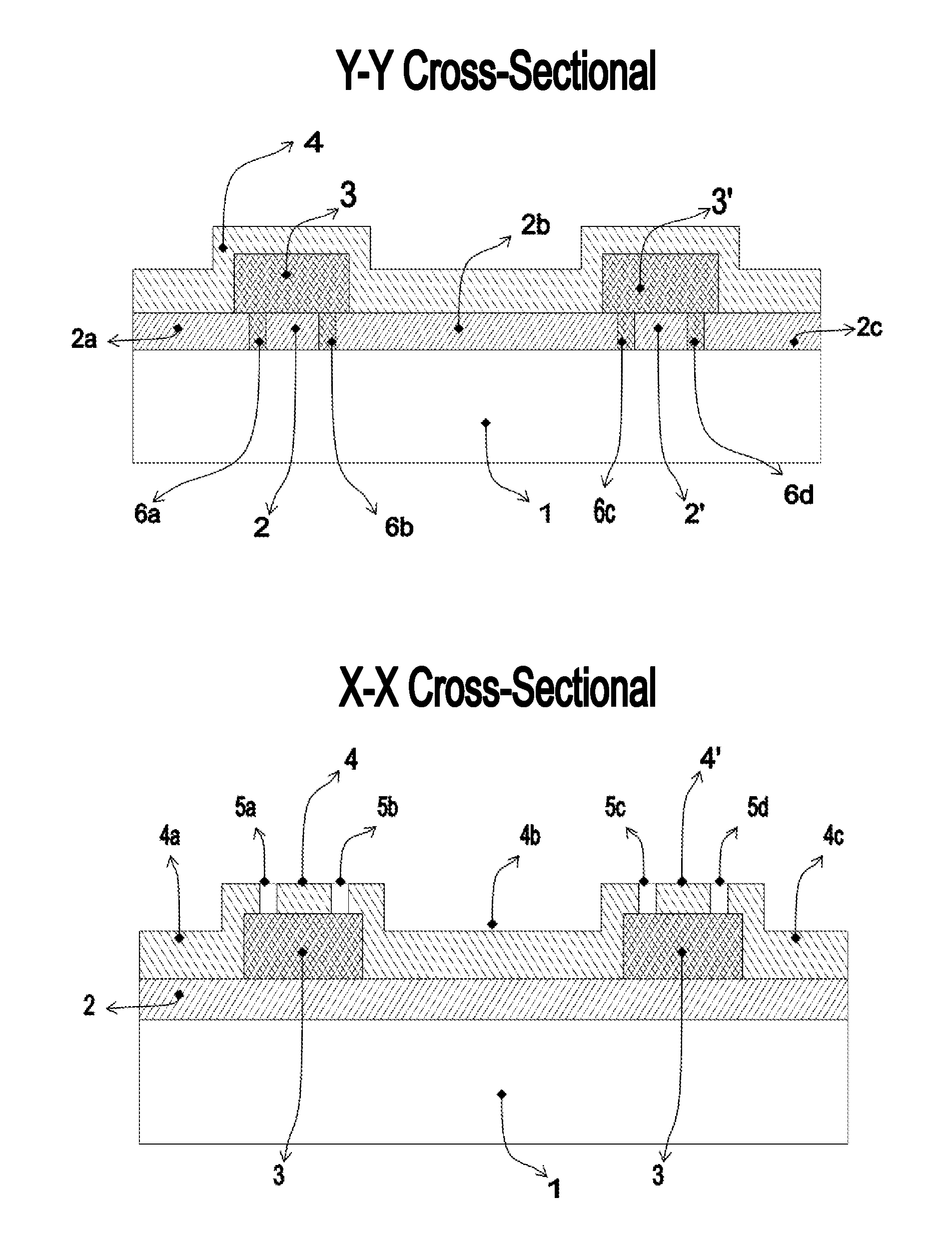
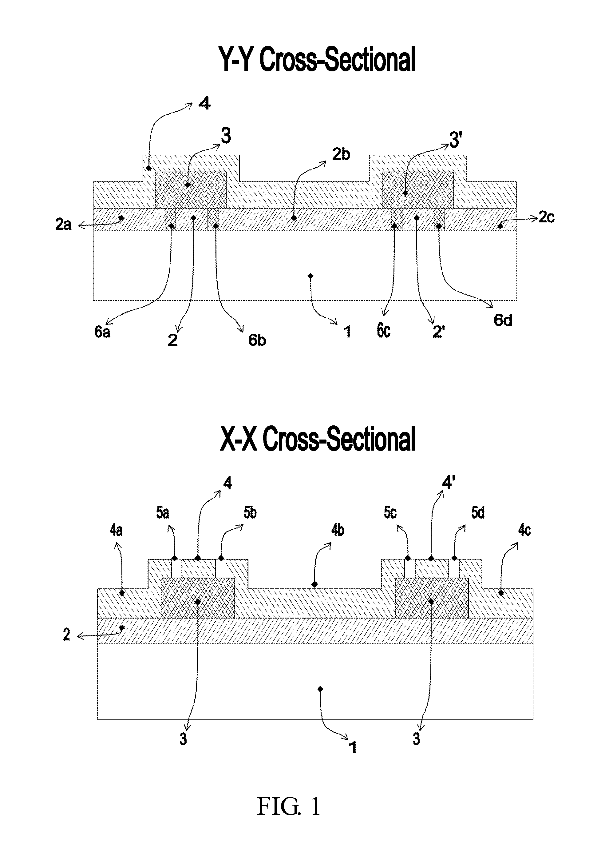
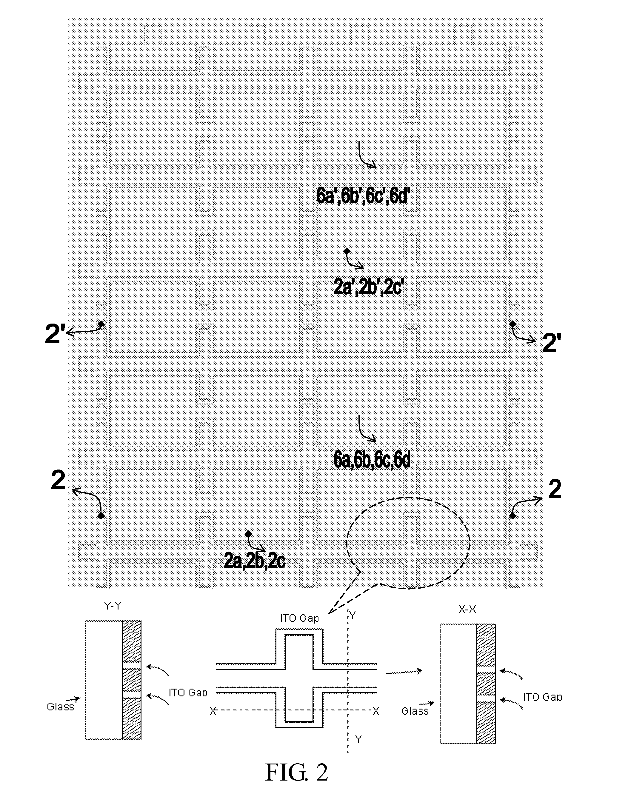
[0042]The first conducting touch function layer is fabricated on a non-conducting substrate by, for example, physical vapor deposition or spray coating, followed by etching using a laser or photolithographic technique to form the insulating gap below the disconnected insulating layer, as shown in FIG. 1, and FIG. 2: 6a, 6b, 6c, 6d and 6a′, 6b′, 6c′, 6d′.
[0043]Insulating blocks, as shown in FIG. 1, and FIG. 3: 3 and 3′, are manufactured by using for example laser or photolithographic etching on the insulating gap of the first conducting touch function layer, as shown in FIG. 1, and FIG...
PUM
 Abstract
Description
Claims
Application Information