
Shared channel masks in on-product test compression system

Inactive Publication Date: 2015-09-10
IBM CORP
View PDF14 Cites 3 Cited by
  • Summary
  • Abstract
  • Description
  • Claims
  • Application Information

AI Technical Summary

Benefits of technology

The present patent is about a semiconductor chip that has on-product test compression, and a design structure for the chip. The chip includes a mask logic that includes a first mask and two channel masks that mask scan channels of a circuit under test. The mask logic also includes comparators that compare the channel mask enable decodes to the channel mask enable encode and produce a channel mask enable encode. The chip also has a memory that stores the channel mask enable decodes for the first and second masks. The technical effect of this design is that it allows for efficient masking of scan channels in a semiconductor chip during on-product testing.

Problems solved by technology

Digital Integrated Circuits (ICs) can be prone to defects introduced during a manufacturing process.
These defects may affect the logic output of the digital IC, which in turn adversely influences semiconductor chip quality and costs.

Method used


Image

  • Shared channel masks in on-product test compression system
  • Shared channel masks in on-product test compression system
  • Shared channel masks in on-product test compression system

Examples


Embodiment Construction

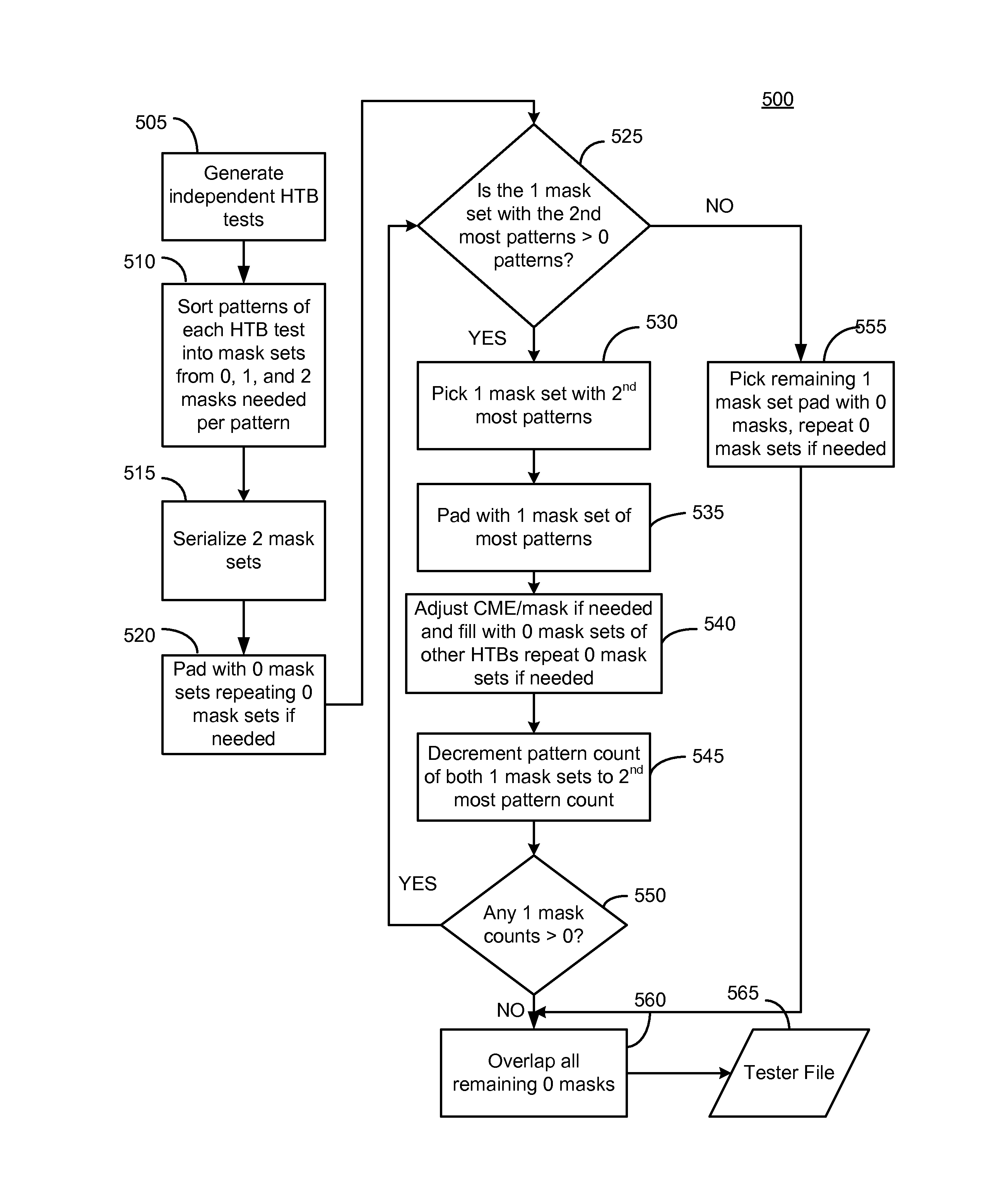
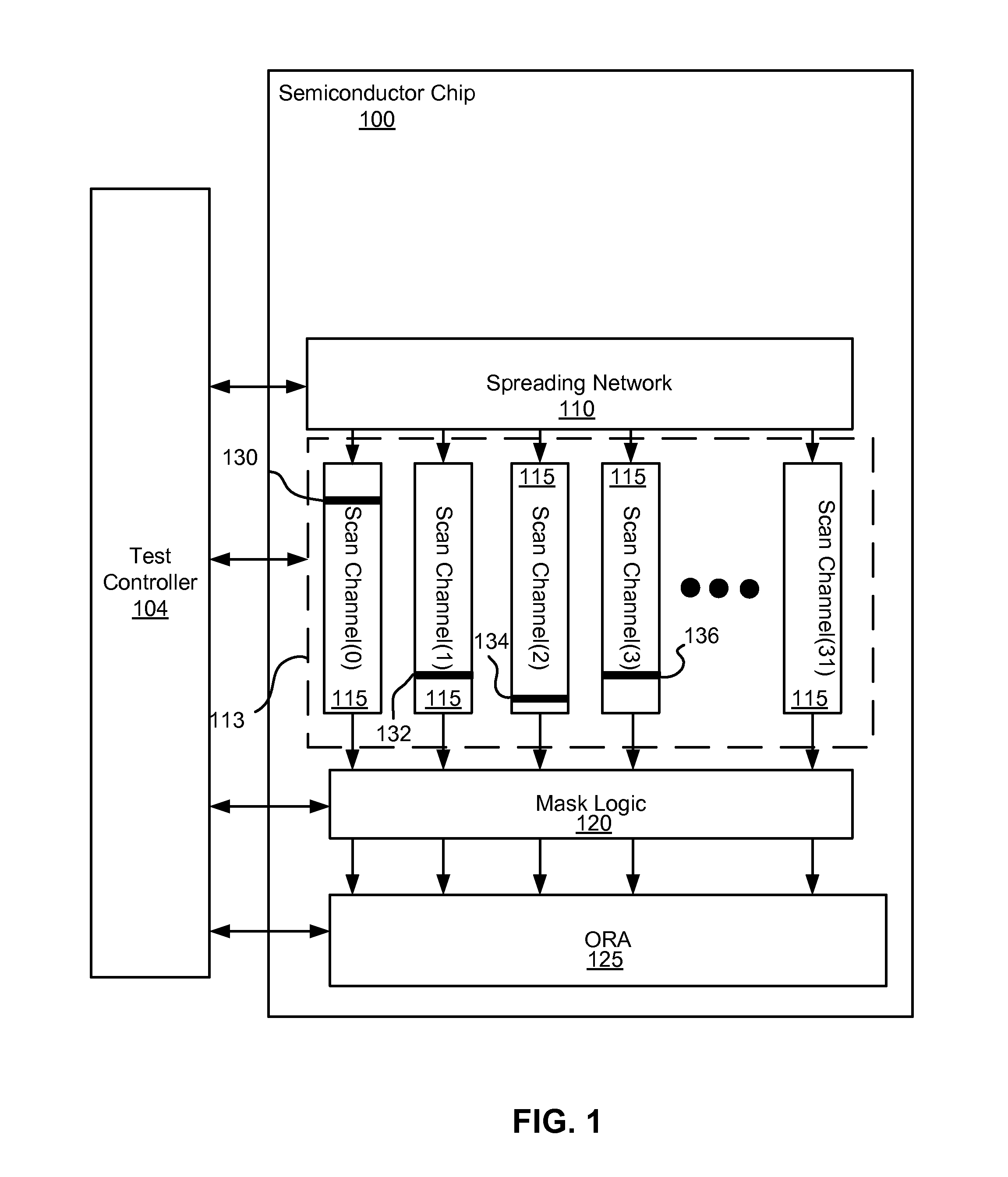
[0020]Aspects of the present disclosure relate to testing electronic components, more particular aspects relate to shared channel masks in an on-product test compression (OPTC) system and a method of sorting and combining test patterns of hierarchal test blocks (HTB) of scan channels to cycle patterns concurrently while minimizing over-masking. A mask is required when a scan channel latch produces and indeterminate also referred to as an X-state result when a test pattern is cycled through it. Masks may be shared between scan channels and HTBs. The sharing may result in over-masking where a mask is enabled for one scan channel or HTB that needs the mask but inadvertently masks good results from other scan channels or HTBs. The method includes creating individual tests for each unique HTB and sorting the patterns of each test into mask sets. The mask sets are defined by the number of masks each pattern requires. The mask sets of each are then combined to run concurrently in a way tha...


PUM


Abstract

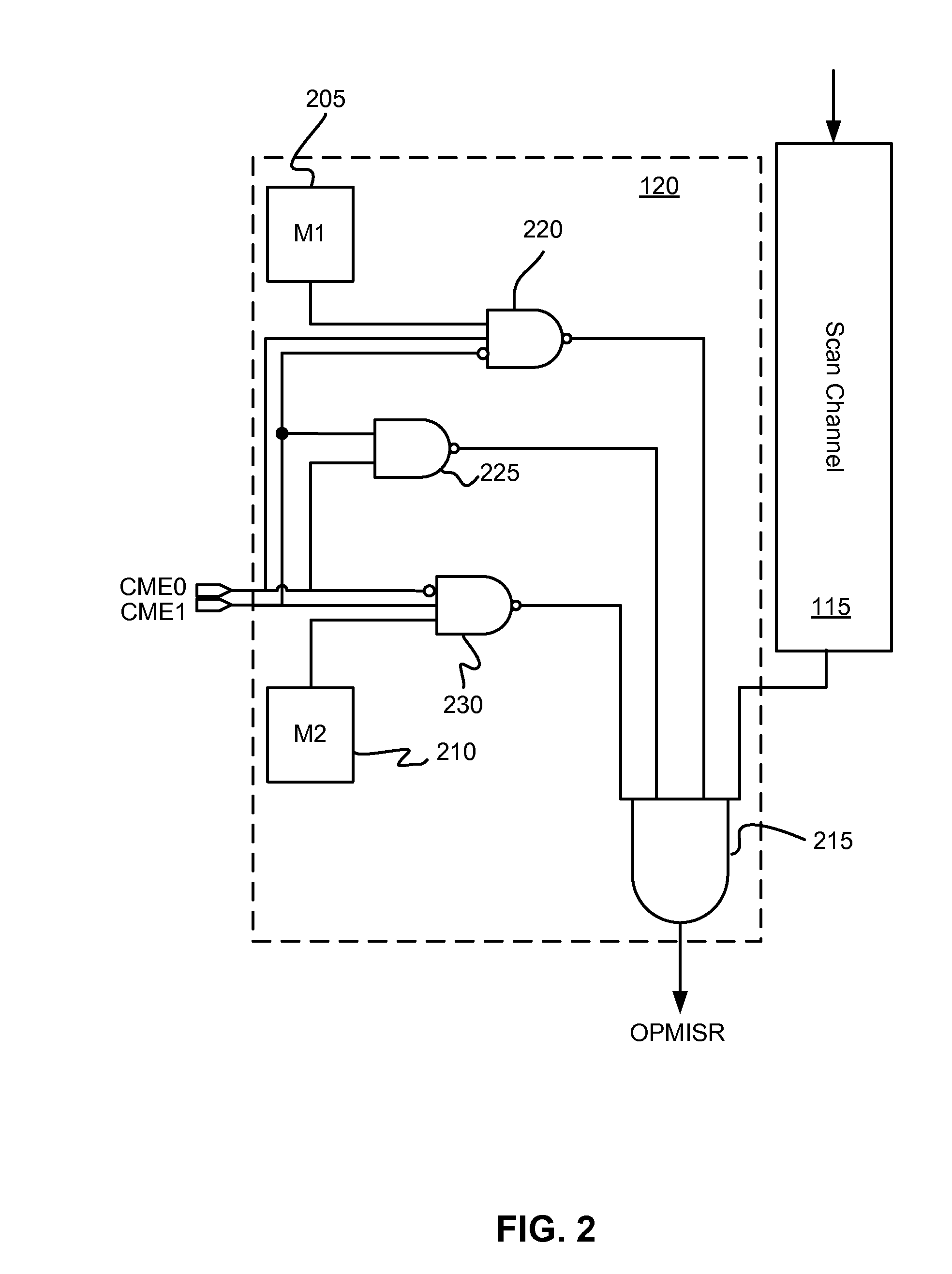
A semiconductor chip includes a first mask logic. The first mask logic includes a first mask and a second mask that mask a respective first scan channel output and a second scan channel output. The first mask logic includes at least three enable pins that receive respective enable signals. The three enable signals produce a channel mask enable encode. The first mask logic includes a first memory that stores a first channel mask enable decode for the first mask and a second memory that stores a second channel mask enable decode for the second mask. The first mask logic includes a first comparator and a second comparator. The first and second comparator compare the respective channel mask enable decodes to the channel mask enable encode. The comparators signal respective masks to mask the respective scan channel when the respective channel mask enable decode matches the channel mask enable encode.

Description

BACKGROUND[0001]The present disclosure relates to testing electronic components, and more specifically, to channel mask sharing in on-product test compression (OPTC) systems.[0002]Digital Integrated Circuits (ICs) can be prone to defects introduced during a manufacturing process. These defects may affect the logic output of the digital IC, which in turn adversely influences semiconductor chip quality and costs. Industry has developed a number of testing techniques to test for the defects. To test for defects, an OPTC network may be built into an IC, allowing the IC to test its own operations. OPTC networks may be implemented using hardware, software, or a combination of the two.SUMMARY[0003]According to embodiments of the present disclosure, a semiconductor chip having on-product test compression is disclosed as well as a design structure of the same. The semiconductor chip includes a first mask logic. The first mask logic includes a first mask and a second mask that mask a respecti...

Claims


Application Information

Patent Timeline
IPC IPC(8): G06F17/50
CPCG06F17/5081G06F30/30G03F1/00G01R31/20G21K5/00G06F21/00G06F30/392G06F30/398G06F30/333G06F2119/18
Inventor DOUSKEY, STEVEN M.KUSKO, MARY P.
Owner IBM CORP
Learn More