Supercharge Your Innovation With Domain-Expert AI Agents!

Elastic positioning structure for a semiconductor carrier

a technology of elastic positioning and semiconductor, applied in the field of semiconductor carriers, can solve the problems of difficult to put in or take out semiconductors, deformation of deformation portions, etc., and achieve the effect of maintaining elastic deformation and recovering the abutting section

Active Publication Date: 2015-09-24
LO YU NAN
View PDF14 Cites 2 Cited by
  • Summary
  • Abstract
  • Description
  • Claims
  • Application Information

AI Technical Summary

Benefits of technology

This patent describes an elastic positioning structure for a semiconductor carrier. The structure includes multiple stop blocks that are formed along the walls of the carrier to maintain its elastic deformability and recoverability. The stop blocks are positioned to securely hold the semiconductor in place. The positioning structure is designed with a narrow top and wide bottom, allowing for easy insertion of the semiconductor into the carrier without disengaging from the stop blocks. The inclined guide surface on the protrusion and the inclined connecting surface on the stop blocks facilitate the insertion of the semiconductor into the recess. These features make the positioning structure efficient in positioning and firmly holding the semiconductor during transportation and processing.

Problems solved by technology

However, the deformation portion 141 still has to provide a push force for the abutting portion 142 to fix the semiconductor, plus the upper width W 1 of the elastic stop block 14 being bigger than the lower width W2 of the elastic stop block 14, as a result, the deformability of the deformation portion 141 is limited, which makes it not easy to put in or take out the semiconductor.

Method used


Image

  • Elastic positioning structure for a semiconductor carrier
  • Elastic positioning structure for a semiconductor carrier
  • Elastic positioning structure for a semiconductor carrier

Examples


Embodiment Construction

[0021]The present invention will be clearer from the following description when viewed together with the accompanying drawings, which show, for purpose of illustrations only, the preferred embodiment in accordance with the present invention.

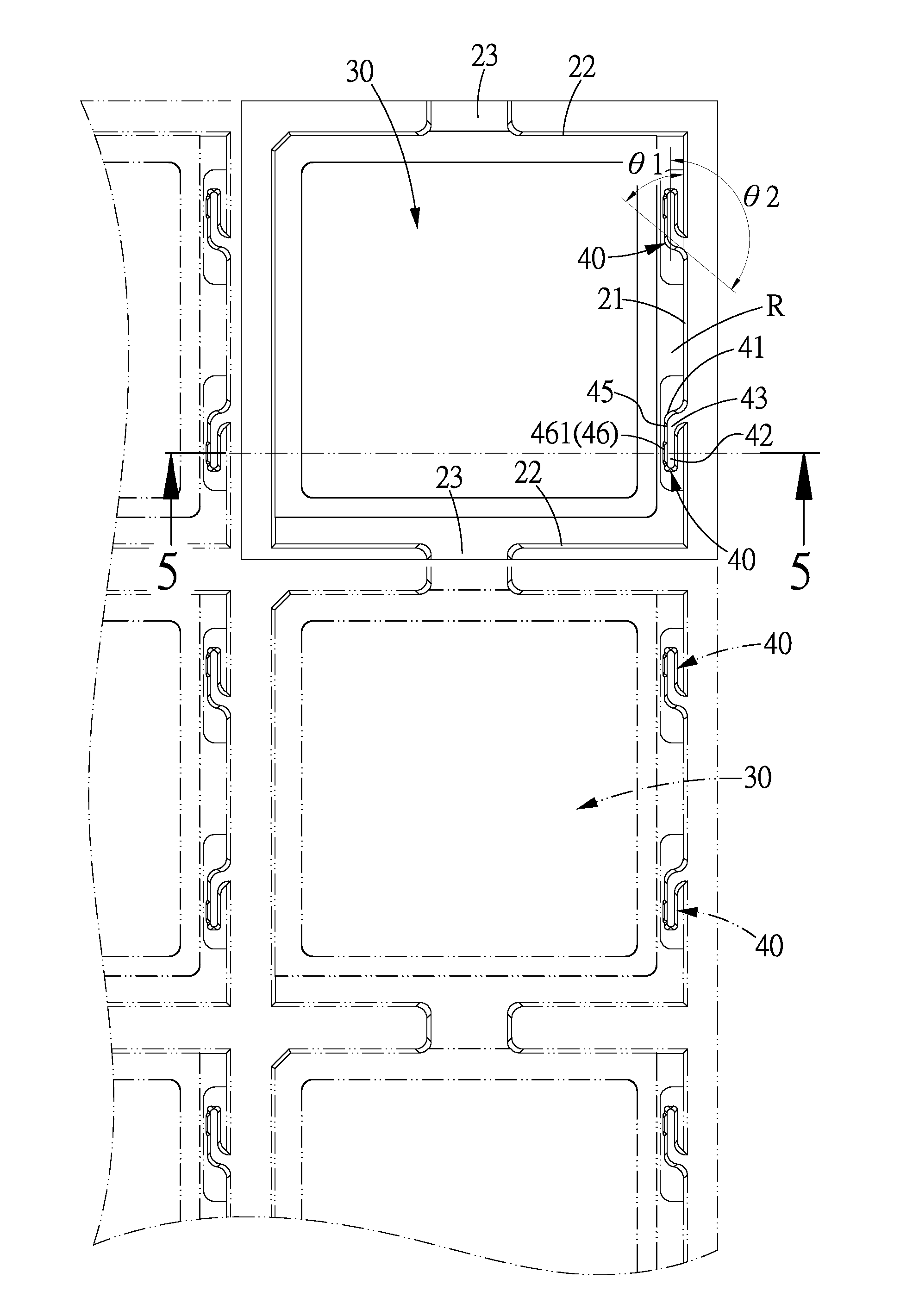
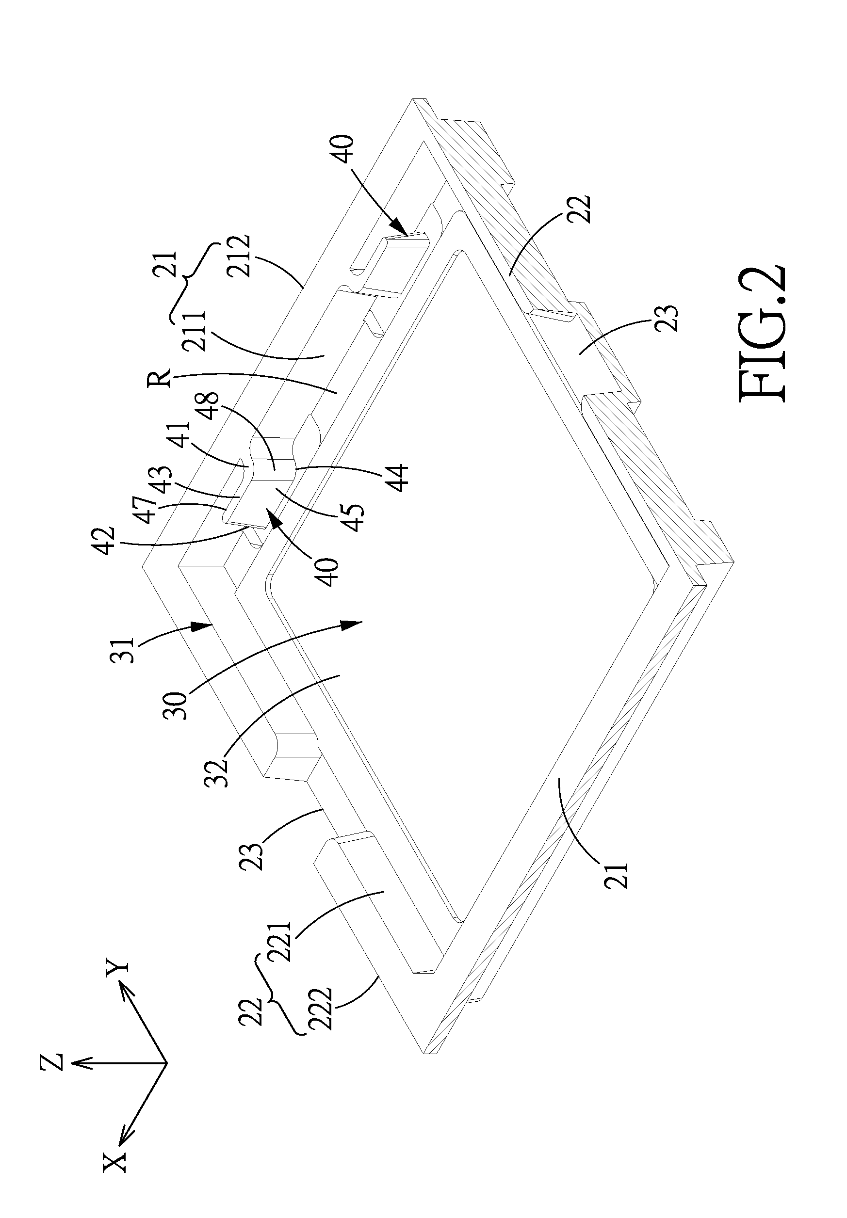
[0022]Referring to FIGS. 2-5, an elastic positioning structure for a semiconductor carrier 20 in accordance with the present invention is shown, wherein the semiconductor carrier 20 comprises a plurality of transversely and longitudinally arranged walls 21, 22, wherein the walls 21 are defined as first walls 21 and the walls 22 are defined as second walls 22 which are perpendicular to the first walls 21.

[0023]The first walls 21 cooperate with the second walls 22 to define a plurality of recesses 30. Each of the recesses 30 includes an opening 31 and a bottom 32 opposite to the opening 31. A direction in which the first walls 21 extend is defined as a direction X, a direction in which the second walls 22 extend is defined as a direction Y, a depth...


PUM


Abstract

An elastic positioning structure for a semiconductor carrier is provided with a plurality of stop blocks formed on and extending along the walls of the semiconductor carrier, the fixed end and the elastic free end of the respective stop blocks are located at the same level, so that the fixed end can still serve as a restricting structure to restrict the semiconductor, even when the free end of the stop blocks lose elasticity. The positioning structure has a narrow top and wide bottom, and the recess of the semiconductor carrier is narrow at the top and wide at the bottom, so that the semiconductor can be easily taken out and put into the recess, and can be well restricted in recess without disengaging therefrom.

Description

[0001]This application is a continuation in part of U.S. patent application Ser. No. 14 / 068,157, which claims the benefit of the earlier filing date of Oct. 31, 2013. Claims 1, 2 and 6 of this application are revised from claims 1, 2 and 6 of the U.S. patent application Ser. No. 14 / 068,157, claim 3 of this application is the same as claim 4 of the U.S. patent application Ser. No. 14 / 068,157, and claims 4 and 5 of this application are new.BACKGROUND OF THE INVENTION[0002]1. Field of the Invention[0003]The present invention relates to a semiconductor carrier, and more particularly to an elastic positioning structure for a semiconductor carrier.[0004]2. Description of the Prior Art[0005]FIG. 1 shows a conventional semiconductor carrier structure 10 includes a plurality of walls 11 arranged in a matrix manner to define a plurality of recesses 12 for holding and protecting semiconductors. For better positioning of micro semiconductor and preventing the semiconductor from disengaging from...

Claims


Application Information

Patent Timeline
IPC IPC(8): B65D1/36
CPCB65D1/36B65D73/02H05K13/0084
Inventor LO, YU-NAN
Owner LO YU NAN
Features
  • R&D
  • Intellectual Property
  • Life Sciences
  • Materials
  • Tech Scout
  • Unparalleled Data Quality
  • Higher Quality Content
  • 60% Fewer Hallucinations
Learn More