Charged-Particle Beam Lithographic System
a lithographic system and charge technology, applied in the direction of electrical discharge tubes, nuclear engineering, electrical apparatus, etc., can solve the problems of deteriorating productivity, difficult to convey the substrate cover by a transport device such as a robot arm, and deteriorating productivity, so as to improve productivity and enhance productivity.
- Summary
- Abstract
- Description
- Claims
- Application Information
AI Technical Summary
Benefits of technology
Problems solved by technology
Method used
Image

Examples
first embodiment
1. First Embodiment
1.1. Configuration of Charged-Particle Beam Lithographic System
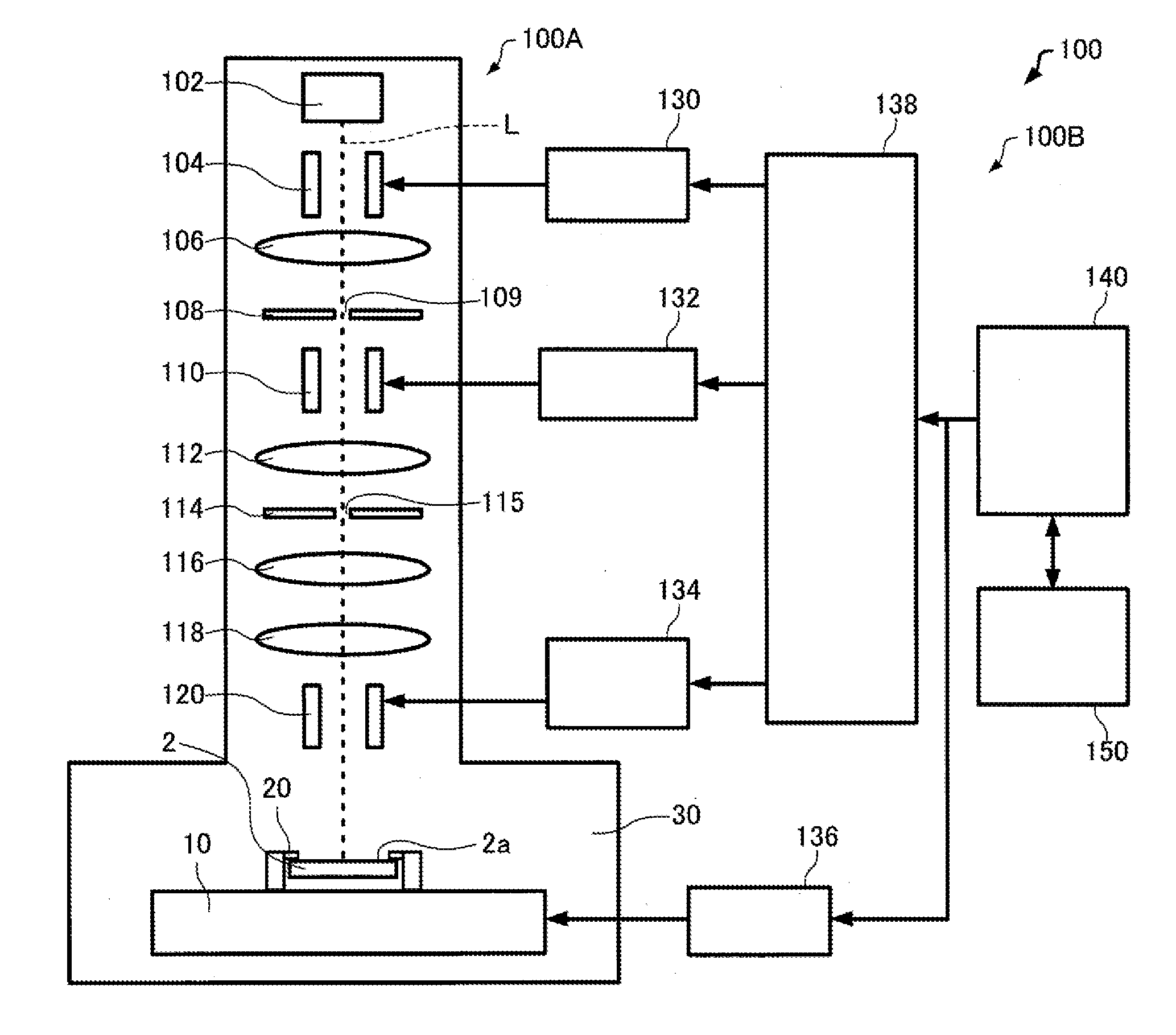
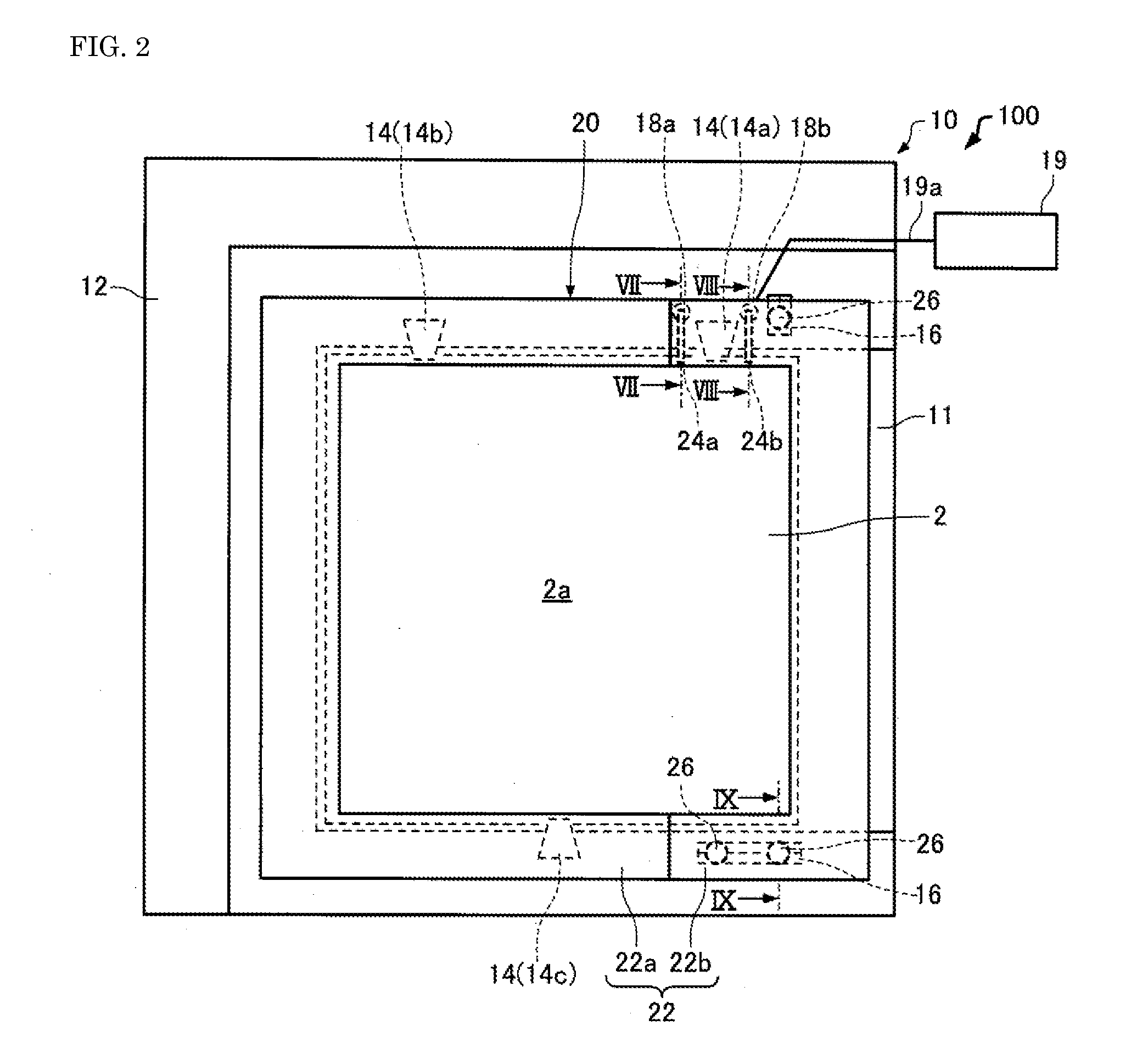
[0044]A charged-particle beam lithographic system, 100, associated with a first embodiment of the present invention is first described by referring to FIG. 1, which schematically shows the configuration of the system 100. In FIG. 1, for the sake of convenience, a substrate stage 10 and a substrate cover 20 are shown in simplified form.
[0045]The charged-particle beam lithographic system 100 is used to write pattern on a substrate 2 by directing a charged particle beam at the substrate. The charged particle beam referred to herein is made of charged particles and includes an electron beam and an ion beam. The substrate 2 can be a mask blank or a semiconductor substrate (such as a silicon substrate).
[0046]As shown in FIG. 1, the charged-particle beam lithographic system 100 includes the substrate stage 10, the substrate cover 20, an electron optical column 100A, and a control section 100B. In the followin...
second embodiment
2. Second Embodiment
[0113]A charged-particle beam lithographic system associated with a second embodiment of the present invention is next described by referring to FIGS. 15 and 16, which are schematic plan views of the substrate stage 10 and the substrate cover 20 of this charged-particle beam lithographic system, 200. FIG. 15 shows a state in which the second part 22b of the frame portion 22 has been mounted over the stage 10. FIG. 16 shows a state in which the second part 22b of the frame portion 22 has been taken out of the stage 10.
[0114]FIG. 17 is a schematic plan view of the second part 22b of the frame portion 22. FIG. 18 is a schematic side elevation of the second part 22b of the frame portion 22. For the sake of convenience, a vibratory portion 210 is shown in simplified form in FIGS. 15, 17, and 18. In FIGS. 15-18, those components of the charged-particle beam lithographic system 200 which are similar in function to their respective counterparts of the above-described cha...
third embodiment
3. Third Embodiment
[0125]A charged-particle beam lithographic system associated with a third embodiment is next described by referring to FIG. 21, which schematically shows the vibratory portion 210 of the system. In FIG. 21, for the sake of convenience, a case 236 is shown to be transparentized.
[0126]The charged-particle beam lithographic system associated with the third embodiment is similar in configuration to the charged-particle beam lithographic system 200 except that the vibratory portion 210 shown in FIG. 21 is different in configuration. Therefore, only the differences with the charged-particle beam lithography system 200 are described below.
[0127]In the charged-particle beam lithographic system 200, the vibratory portion 210 vibrates the second part 22b of the frame portion 22 by rotating the eccentric weight 212 using the motor 214 as shown in FIG. 19.
[0128]On the other hand, in the charged-particle beam lithographic system associated with the third embodiment, the vibrat...
PUM
 Abstract
Description
Claims
Application Information
 - R&D Engineer
- R&D Manager
- IP Professional
- Industry Leading Data Capabilities
- Powerful AI technology
- Patent DNA Extraction
Browse by: Latest US Patents, China's latest patents, Technical Efficacy Thesaurus, Application Domain, Technology Topic.
© 2024 PatSnap. All rights reserved.Legal|Privacy policy|Modern Slavery Act Transparency Statement|Sitemap