Array Substrate for Display Device and Manufacturing Method Thereof

Active Publication Date: 2015-10-22
LG DISPLAY CO LTD
View PDF3 Cites 21 Cited by
  • Summary
  • Abstract
  • Description
  • Claims
  • Application Information

AI Technical Summary

Benefits of technology

[0022]According to an embodiment of the present invention, a transparent electrode pattern for increasing adhesion strength may be formed between an S/D metal layer and a passivation layer located above the S/D metal layer in an inorganic passivation hole (PAS hole) area or an organic passivation hole (PAC hole) area formed on a metal pattern such as the S/D metal layer. Accordingly, it may be possible to prevent display failure due to a delamination phenomenon or peel-off of a material of a passivation layer, which are caused by the lack of adhesion strength of a metal layer and the passivation layer in the passivation hole area.
[0023]For example, use is made of an organic insulating layer or an organic passivation layer (PAC) formed of an organic material, such as photo-acr

Problems solved by technology

However, an LCD device of the above-described TN mode may be disadvantageous due to its narrow viewing angle of about 90 degrees.
For example, when the foreign material generated from the passi

Method used


Image

  • Array Substrate for Display Device and Manufacturing Method Thereof
  • Array Substrate for Display Device and Manufacturing Method Thereof
  • Array Substrate for Display Device and Manufacturing Method Thereof

Examples


Example

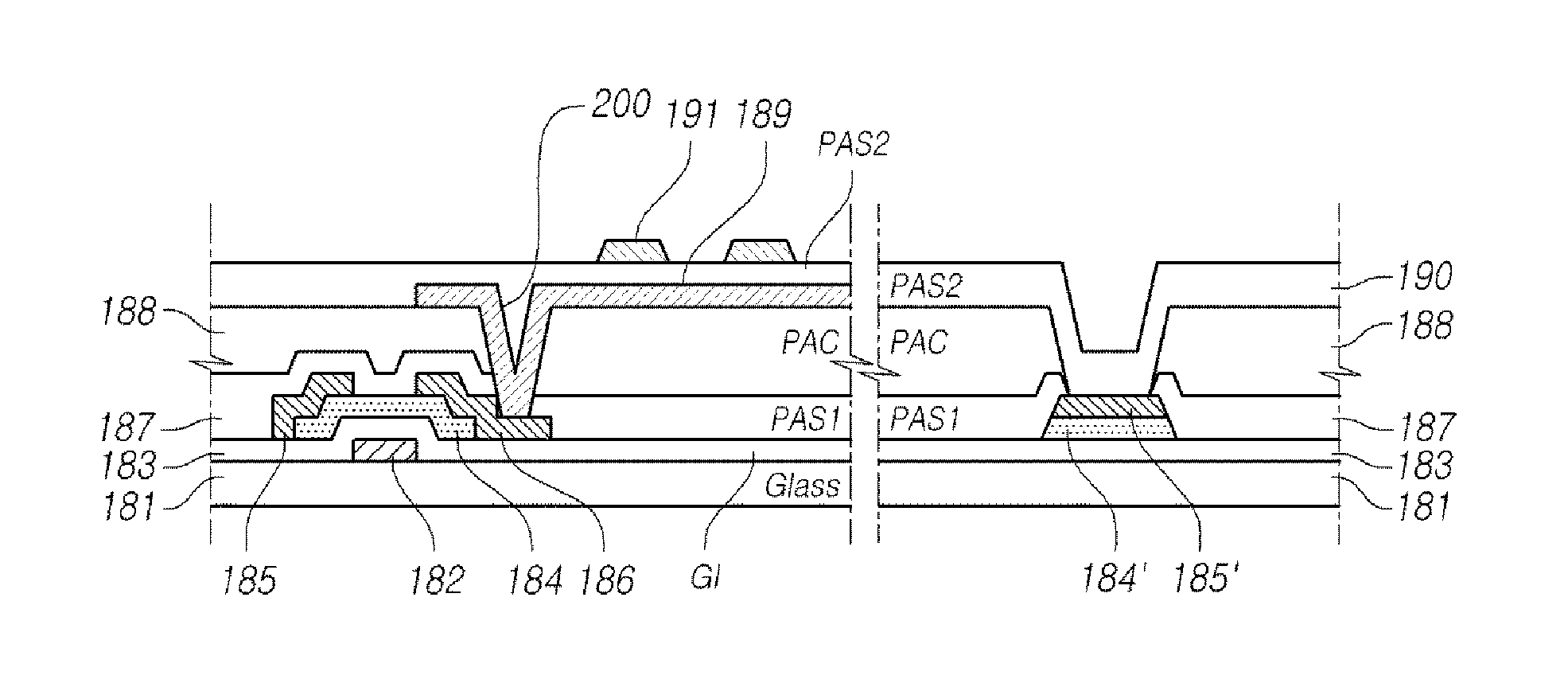
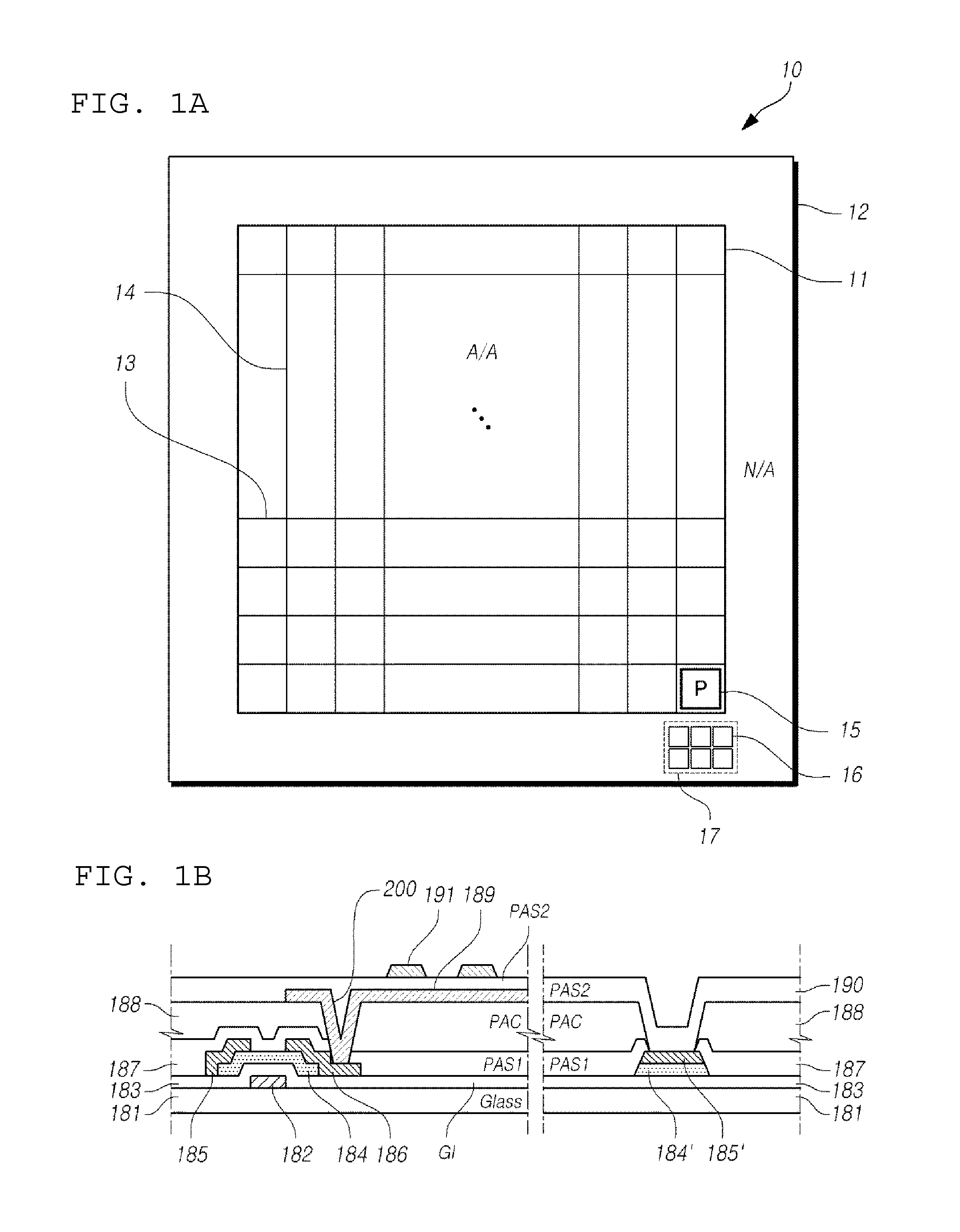
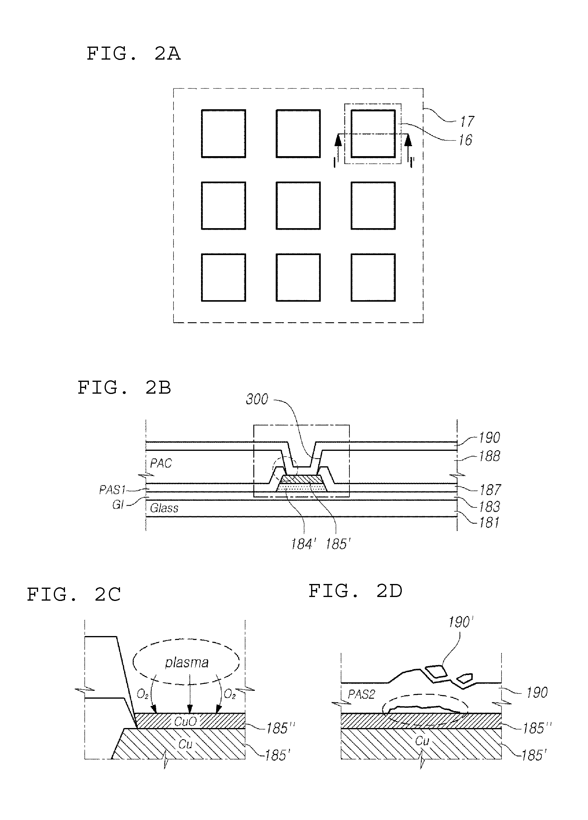
[0031]Hereinafter, embodiments of the present invention will be described in detail with reference to the accompanying drawings. In the following description, the same or similar elements will be designated by the same reference numerals to indicate the same or similar parts. Further, in the following description of embodiments of the present invention, a detailed description of known functions and configurations incorporated herein may be omitted when it may make the subject matter of embodiments of the present invention rather unclear.

[0032]In addition, terms such as first, second, A, B, (a), (b) or the like may be used herein when describing components of embodiments of the present invention. Each of these terminologies is not used to define an essence, order or sequence of a corresponding component but used merely to distinguish the corresponding component from other component(s). In the case that it is described that a certain structural element “is connected to”, “is coupled t...


PUM


Abstract

The present disclosure provides an array substrate for a display device and a manufacturing method thereof. A transparent electrode pattern (ITO) may be formed between a source/drain metal pattern and a passivation layer located above the source/drain metal pattern, which are formed in a passivation hole area of a non-active area of the array substrate. Accordingly, it may be possible to prevent display failure caused by a delamination phenomenon or peel-off of a material of the passivation layer due to the lack of adhesion strength between a metal layer and the passivation layer in the passivation hole area.

Description

CROSS-REFERENCE TO RELATED APPLICATION[0001]This application claims priority from and the benefit of Korean Patent Application No. 10-2014-0046151, filed on Apr. 17, 2014, which is hereby incorporated by reference for all purposes as if fully set forth herein.BACKGROUND[0002]1. Field of the Invention[0003]Embodiments of the present invention relate to an array substrate for a display device and a manufacturing method thereof. More particularly, the embodiments of the present invention relate to an array substrate for a display device and a manufacturing method thereof, which can prevent problems due to the damage of a passivation layer in a passivation hole area formed on a Source / Drain (S / D) metal pattern in a non-active area.[0004]2. Description of the Related Art[0005]With the progress of an information-oriented society, demands for display devices for displaying images have increased in various forms. Recently, various display devices, such as a Liquid Crystal Display (LCD), a P...

Claims


Application Information

Patent Timeline
IPC IPC(8): H01L23/31H01L29/423H01L21/283H01L23/29H01L29/417H01L29/786H01L29/66H01L21/311H01L27/12H01L21/3213
CPCH01L23/3192H01L27/124H01L29/42384H01L27/1259H01L21/283H01L21/32133H01L2021/775H01L29/78669H01L29/66765H01L21/31111H01L23/293H01L23/291H01L21/31133H01L29/41733G02F1/133345G02F1/13458H01L2924/0002H01L2924/00H01L29/78618G02F1/134372G02F1/134363G02F1/13439G02F1/1368G02F2201/121G02F2201/123H01L21/84H01L27/1222H01L27/1244H01L27/1248H01L27/127
Inventor CHOI, SUNHYUNSHIN, KITAEGJO, CHELHEEROH, TAEYUN
Owner LG DISPLAY CO LTD
Why Eureka
Try Eureka