Semiconductor device and method for manufacturing the same

a technology of semiconductors and semiconductors, applied in the direction of semiconductor devices, electrical devices, transistors, etc., can solve the problems of inconsistency in device performance across the wafer and too long response time of the devi

Active Publication Date: 2015-10-22
INST OF MICROELECTRONICS CHINESE ACAD OF SCI
View PDF5 Cites 20 Cited by
  • Summary
  • Abstract
  • Description
  • Claims
  • Application Information

AI Technical Summary

Problems solved by technology

Unfortunately, it is difficult to control fins formed on a wafer to have the same height during manufacture of an integrated circuit (IC), resulting in inconsistency in performance of devices across the wafer.
If the parasitic capacitance is too large, the response time of the device will become too long.

Method used


Image

  • Semiconductor device and method for manufacturing the same
  • Semiconductor device and method for manufacturing the same
  • Semiconductor device and method for manufacturing the same

Examples


Embodiment Construction

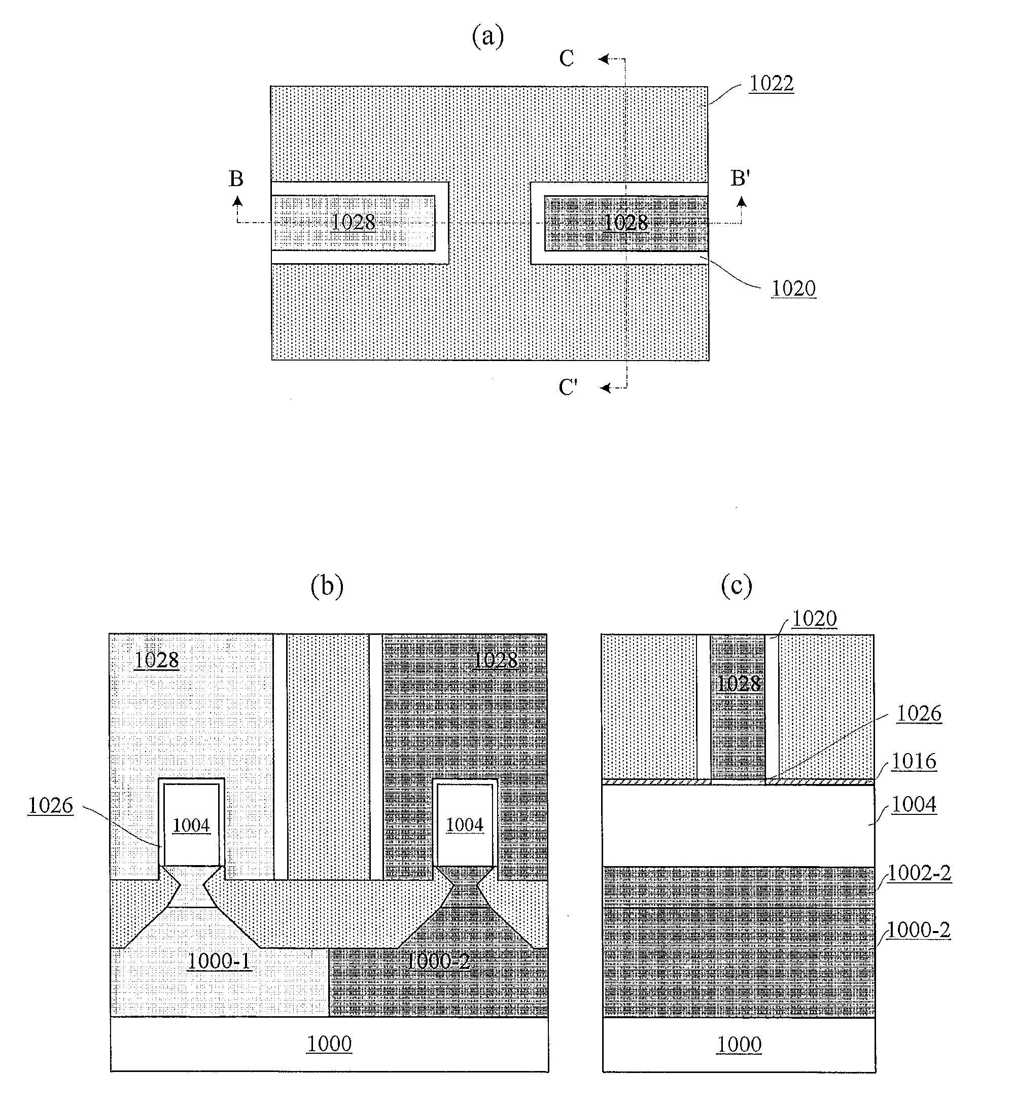
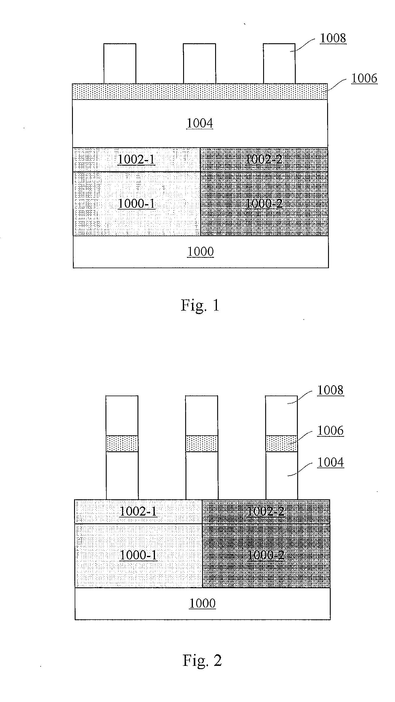
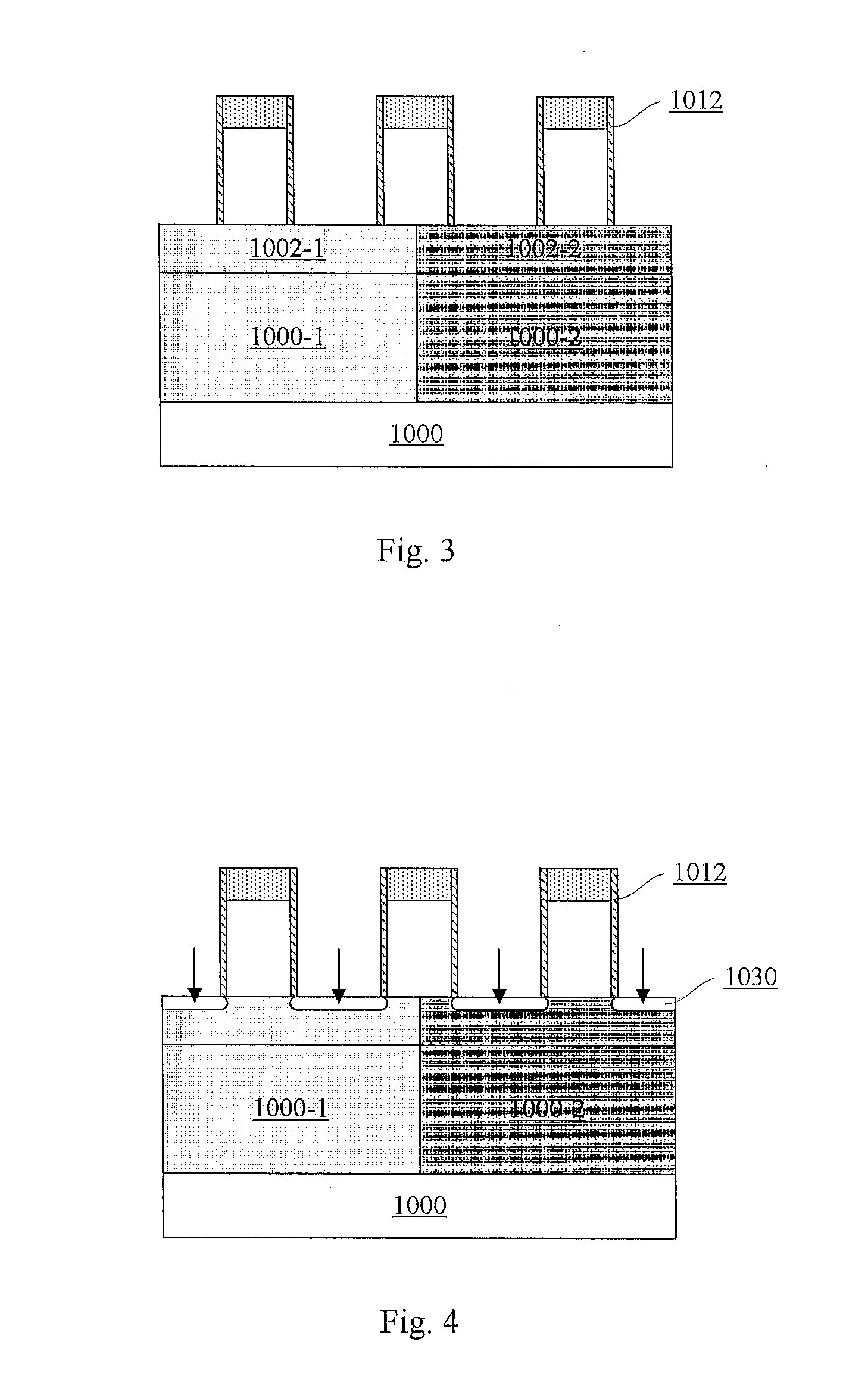
[0010]Hereinafter, the technology disclosed herein is described with reference to embodiments thereof shown in the attached drawings. However, it should be noted that those descriptions are just provided for illustrative purpose, rather than limiting the present disclosure. Further, in the following, descriptions of known structures and techniques are omitted so as not to obscure the concept of the present disclosure.

[0011]In the drawings, various structures according to the embodiments are schematically shown. However, they are not drawn to scale, and some features may be enlarged while some features may be omitted for sake of clarity. Moreover, shapes and relative sizes and positions of regions and layers shown in the drawings are also illustrative, and deviations may occur due to manufacturing tolerances or technique limitations in practice. Those skilled in the art can also devise regions / layers of other different shapes, sizes, and relative positions as desired.

[0012]In the con...


PUM


Abstract

A semiconductor device and a method for manufacturing the same, wherein an example method may include: forming a first semiconductor layer and a second semiconductor layer sequentially on a substrate; patterning the second semiconductor layer to form an initial fin; performing anisotropic etching on the first semiconductor layer to form a Σ-shaped lateral recess therein; forming an isolation layer on the substrate to have a portion that fills the lateral recess, wherein the isolation layer, except the portion that fills the lateral recess, has a top surface located between a top surface and a bottom surface of the first semiconductor layer, and thus defines a fin above the isolation layer; and forming a gate stack intersecting the fin on the isolation layer.

Description

CROSS-REFERENCE TO RELATED APPLICATION[0001]This application claims priority to Chinese Patent Application No. 201210447834.8, filed on Nov. 9, 2012, entitled “Semiconductor Device and Method for Manufacturing the Same,” which is incorporated herein by reference in its entirety.TECHNICAL FIELD[0002]The present disclosure relates to semiconductor technology, and particularly to semiconductor devices and methods for manufacturing the same.BACKGROUND[0003]Short channel effects are getting more significant as planar semiconductor devices are increasingly being scaled down. To this end, three-dimensional (3D) semiconductor devices, such as Fin Field Effect Transistors (FinFETs), have been proposed. Generally, a FinFET includes a fin formed vertically on a substrate and a gate stack intersecting the fin. As such, a channel is formed in the fin, and has a width defined basically by a height of the fin. Unfortunately, it is difficult to control fins formed on a wafer to have the same height...

Claims


Application Information

Patent Timeline
Patent Type & Authority Applications(United States)
IPC IPC(8): H01L27/088H01L29/161H01L29/06H01L21/311H01L21/8234H01L21/306H01L21/265H01L29/16H01L21/02
CPCH01L27/0886H01L29/16H01L29/161H01L29/0653H01L21/02532H01L21/02274H01L21/823481H01L21/30604H01L21/265H01L21/31111H01L21/823431H01L21/823821H01L27/0924H01L21/30608H01L21/823878H01L29/0673H01L29/785
Inventor ZHU, HUILONG
Owner INST OF MICROELECTRONICS CHINESE ACAD OF SCI
Why Eureka
Try Eureka