Thin film transistor, array substrate and method for fabricating the same, and display device

a thin film transistor and array substrate technology, applied in the field of display technology, can solve problems such as deterioration of the performance of pixel elements or thin film transistors, and achieve the effects of preventing deterioration of the performance of the semiconductor active layer, avoiding the increase of the number of patterning processes, and ensuring the performance of thin film transistors

Active Publication Date: 2015-10-22
BOE TECH GRP CO LTD
View PDF6 Cites 15 Cited by
  • Summary
  • Abstract
  • Description
  • Claims
  • Application Information

AI Technical Summary

Benefits of technology

[0021]Since the first transparent electrode is provided between the source electrode and the semiconductor active layer and the second transparent electrode is provided between the drain electrode and the semiconductor active layer, and the first and second transparent electrodes function as a conductive spacer layer. Therefore, when metal atoms (e.g., copper atoms) in the source metal electrode and the drain metal electrode diffuse, they diffuse into the first transparent electrode and the second transparent electrode, rather than diffusing into the semiconductor active layer. That is, the first transparent electrode and the second transparent electrode stop copper atoms from diffusing into the semiconductor active layer, which may prevent deterioration of performance of the semiconductor active layer, so that performance of the thin film transistor is ensured. In addition, during fabrication of an array substrate comprising the thin film transistor, since the first transparent electrode, the second transparent electrode, the source electrode and the drain electrode are formed by one patterning process, increment in numbers of the patterning processes can be avoided.

Problems solved by technology

However, when this kind of metal (e.g., copper) is used for wiring or serves as an electrode, the metal is likely to diffuse into adjacent circuit elements or semiconductor layer in the thin film transistor, resulting in deterioration of performance of pixel elements or thin film transistors.

Method used


Image

  • Thin film transistor, array substrate and method for fabricating the same, and display device
  • Thin film transistor, array substrate and method for fabricating the same, and display device
  • Thin film transistor, array substrate and method for fabricating the same, and display device

Examples


Embodiment Construction

[0037]Hereinafter, the technical solutions in the embodiments of the present invention will be described clearly and completely with reference to the accompanying drawings in the embodiments. Obviously, the described embodiments are only a part but not all of the embodiments of the present invention. All other embodiments obtained by a person skilled in the art without creative efforts fall within the protection scope of the present invention.

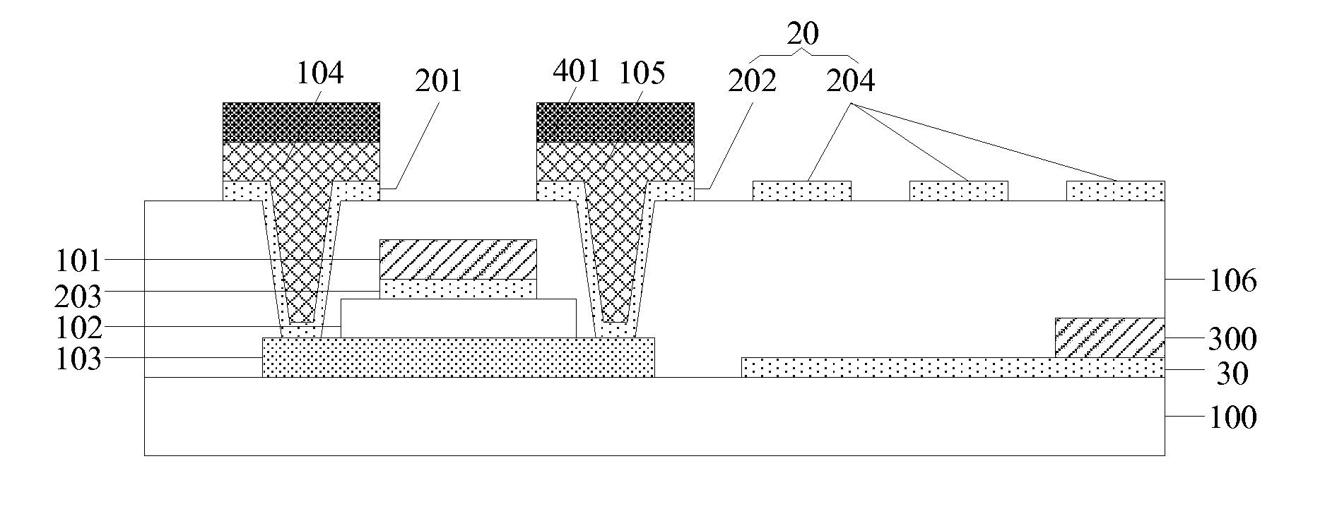
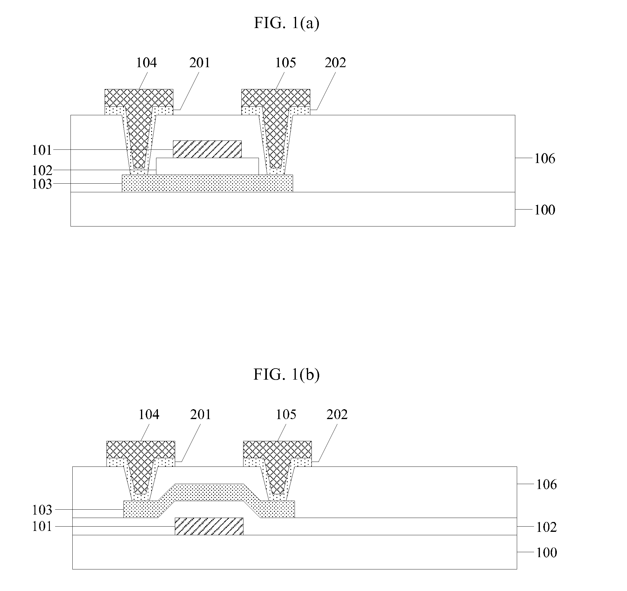
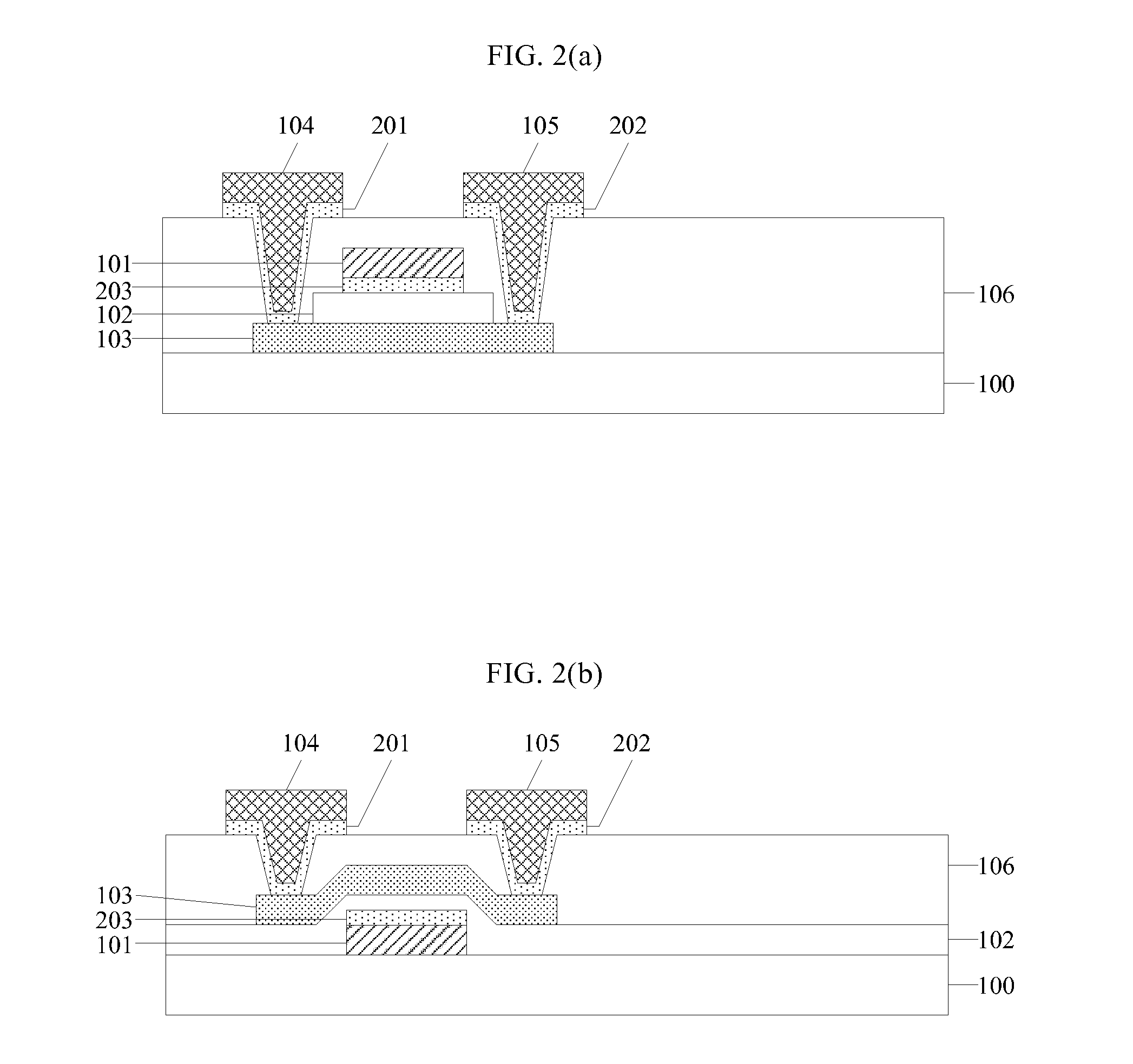
[0038]The embodiments of the present invention provide a thin film transistor, which, as shown in FIGS. 1(a) and 1(b), comprises a gate electrode 101, a gate insulation layer 102, a semiconductor active layer 103, a source electrode 104, a drain electrode 105 and a protection layer 106 which are provided on a base substrate 100. The thin film transistor further comprises: a first transparent electrode 201 that is provided between the source electrode 104 and the semiconductor active layer 103, corresponds to the source electrode 104 and is in d...


PUM


Abstract

A thin film transistor, an array substrate and a method for fabricating the array substrate, and a display device are disclosed. The thin film transistor comprises a gate electrode, a gate insulation layer, a semiconductor active layer, a source electrode, a drain electrode and a protection layer provided on a base substrate, and comprises: a first transparent electrode provided between the source electrode and the semiconductor active layer, corresponding to the source electrode and in direct contact with the source electrode; a second transparent electrode provided between the drain electrode and the semiconductor active layer, corresponding to the drain electrode and in direct contact with the drain electrode, the first transparent electrode is in contact with the semiconductor active layer through a first via provided in the protection layer, the second transparent electrode is in contact with the semiconductor active layer through a second via provided in the protection layer.

Description

FIELD OF THE INVENTION[0001]The present invention relates to the field of display technology, and more particularly, to a thin film transistor, an array substrate and a method for fabricating the array substrate, and a display device.BACKGROUND OF THE INVENTION[0002]In the field of display technology represented by liquid crystal displays (referred to as LCDs), due to improved resolution, increased display size and low resistance wiring required in integrating driver circuits in a display device, wires and electrodes, such as gate lines, and data lines as well as gate electrodes, source electrodes and drain electrodes in thin film transistors (referred to as TFTs), which are made of metal with low resistance characteristics (e.g., copper) have already been applied to the display devices. However, when this kind of metal (e.g., copper) is used for wiring or serves as an electrode, the metal is likely to diffuse into adjacent circuit elements or semiconductor layer in the thin film tr...

Claims


Application Information

Patent Timeline
Patent Type & Authority Applications(United States)
IPC IPC(8): H01L27/12H01L29/417H01L29/49H01L29/786H01L29/45
CPCH01L27/1225H01L29/7869H01L27/1248H01L29/41758H01L29/4908H01L29/4966H01L29/41733H01L29/45H01L27/1214H01L27/1259H01L29/78666H01L29/78669G02F1/1368H01L27/12G02F1/136227H01L29/66969H01L27/124H01L27/1288G02F1/13629H01L29/786
Inventor NING, CE
Owner BOE TECH GRP CO LTD
Why Eureka
Try Eureka