Wafer mapping apparatus and load port including same

a mapping apparatus and load port technology, applied in the field of wafer mapping apparatus, can solve the problem of colliding with a slightly protruding wafer, and achieve the effect of restrainting the generation of abrasion powder which contaminates the processing room

Active Publication Date: 2015-10-29
SINFONIA TECHNOLOGY CO LTD
View PDF0 Cites 3 Cited by
  • Summary
  • Abstract
  • Description
  • Claims
  • Application Information

AI Technical Summary

Benefits of technology

[0015]To put it differently, a protruding wafer which may collide with the mapping sensor is detected by the first protrusion sensor, whereas a protruding wafer which may collide with the first protrusion sensor which moves in front of the mapping sensor is detected by the second protrusion sensor. This allows a load port dealing with differently-sized wafers to be able to employ a common wafer mapping apparatus, while preventing the collision of a wafer with the mapping sensor and / or the protrusion sensor. In addition to the above, because in this wafer mapping apparatus the number of a actuators in one mapping device is small, the generation of abrasion powder which contaminates a processing room is restrained.
[0017]Because the distance between the first protrusion sensor and the mapping sensor is arranged to be equal to or longer than the braking distance in the up-down moving direction of the mapping device, collision of the mapping sensor with a wafer is certainly prevented.
[0018]Because the irradiation axis of the second protrusion sensor is, at a central portion in a left-right direction of the front opening span of each of the containers, arranged to be farther from the containers than the radiation axis of the first protrusion sensor, collision of the second protrusion sensor with a wafer is prevented.
[0020]In the wafer mapping apparatus of the present invention, a protruding wafer which may collide with the mapping sensor is detected by the first protrusion sensor, whereas a protruding wafer which may collide with the first protrusion sensor which moves in front of the mapping sensor is detected by the second protrusion sensor. This allows a load port dealing with differently-sized wafers to be able to employ a common wafer mapping apparatus, while preventing the collision of a wafer with the mapping sensor and / or the protrusion sensor. In addition to the above, because in this wafer mapping apparatus the number of a actuators in one mapping device is small, the generation of abrasion powder which contaminates a processing room is restrained.

Problems solved by technology

On this account, as described in Patent Literatures 1 and 3, the transmission optical sensor which is attached to the fixed frame of the door of the load port so that the optical axis of the sensor extends in the up-down direction cannot be employed as the protrusion sensor, because this sensor is not able to detect a wafer W1 which slightly protrudes in the container.
However, this protrusion sensor, which moves in the up-down direction in the container, may itself collide with a slightly-protruding wafer.

Method used


Image

  • Wafer mapping apparatus and load port including same
  • Wafer mapping apparatus and load port including same
  • Wafer mapping apparatus and load port including same

Examples


Embodiment Construction

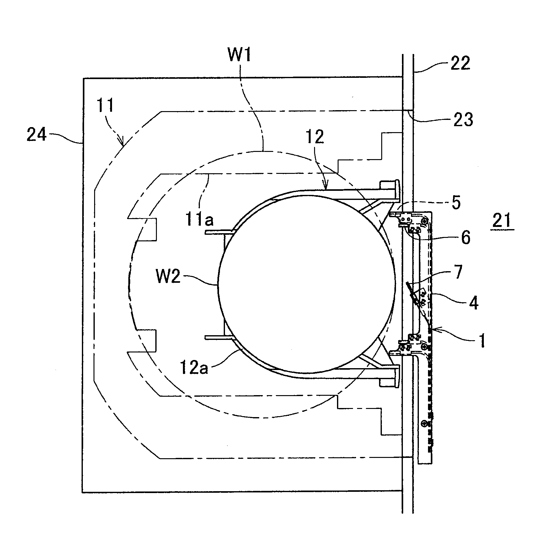
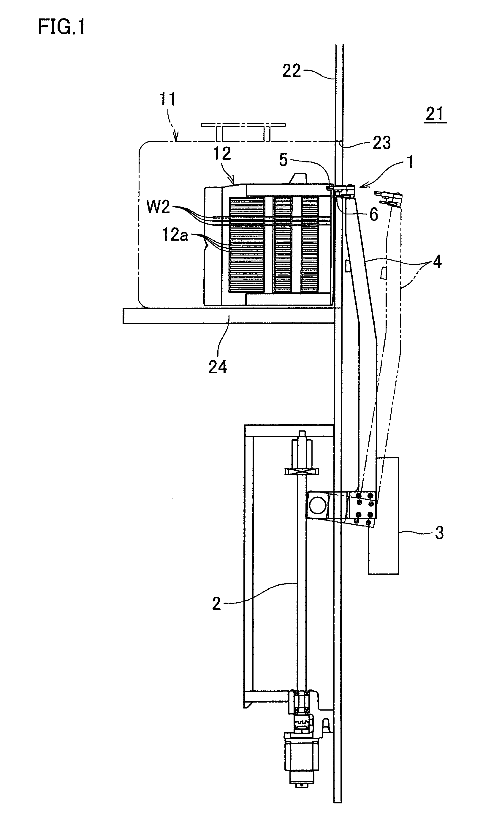
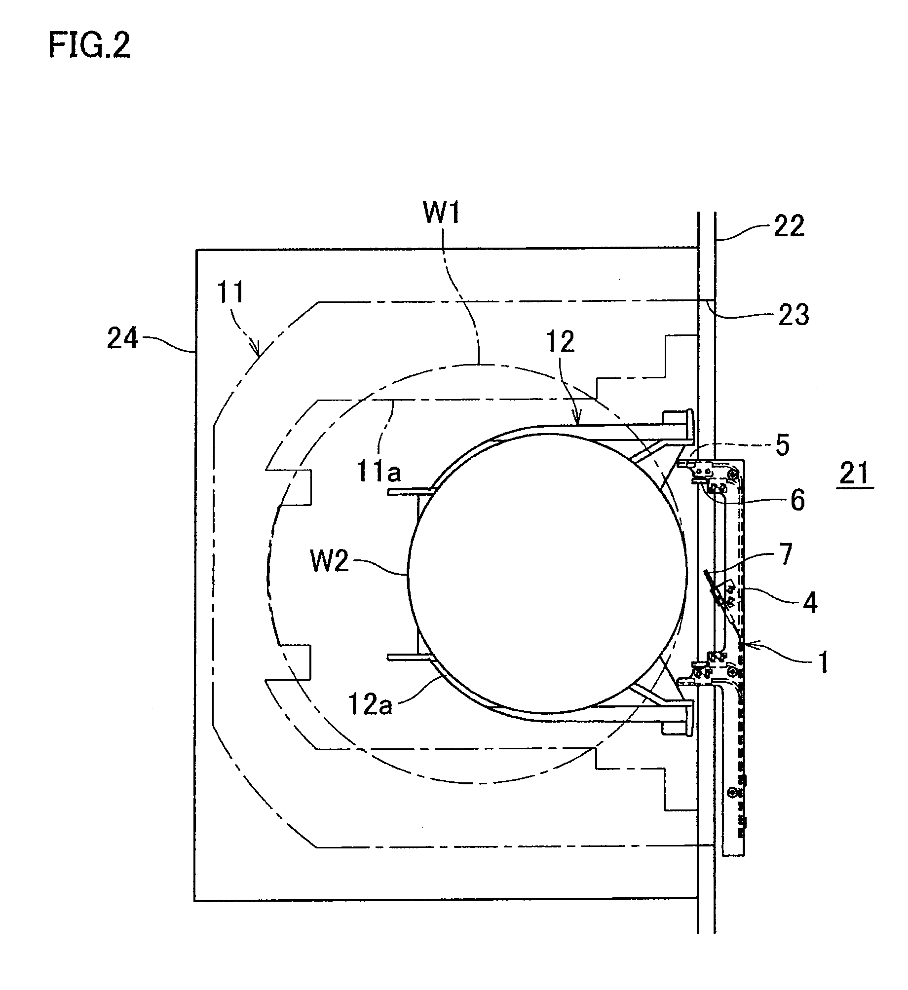
[0026]The following will describe an embodiment of the present invention with reference to figures. FIG. 1 and FIG. 2 show a load port of the present invention, which includes a wafer mapping apparatus 1. This load port deals with both wafers W1 which are stored in a FOUP 11 and 300 mm in diameter and wafers W2 which are stored in an open cassette 12 and 200 mm in diameter. In this load port, a table 24 on which the conveyed FOUP 11 and / or open cassette 12 is placed is provided in front of an entrance 23 formed through a shielding wall 22 of a processing room 21 which is arranged to be a clean environment.

[0027]In FIG. 1 and FIG. 2, a case where the wafers W2 which are stored in the open cassette 12 and 200 mm in diameter are dealt with is indicated by full lines, whereas a case where the wafers W1 which are stored in the FOUP 11 and 300 mm in diameter are dealt with is indicated by dashed lines. The wafers W1 and W2 are stored in vertically-aligned shelves 11a and 12a of the FOUP 1...


PUM


Abstract

The left-right span between a light projection section 5a and a light receiving section 5b of a mapping sensor 5 having an optical axis L1 extending in a left-right horizontal direction is arranged to be narrower than the span of a front opening of a open cassette 12 which is a smaller one of differently-sized containers conveyed to a load port, and the mapping sensor is attached to a mapping device 4. A first protrusion sensor 6 having an optical axis L2 extending in the left-right horizontal direction is attached to the mapping device 4 to be separated from the mapping sensor 5 in a moving direction of the mapping sensor 5. Furthermore, a second protrusion sensor 7 having an optical axis extending in the up-down moving direction of the mapping sensor 5 is provided.

Description

CROSS REFERENCE TO RELATED APPLICATION[0001]The present application claims priority from Japanese Patent Application No. 2014-092924, which was filed on Apr. 28, 2014, the disclosure of which is herein incorporated by reference in its entirety.BACKGROUND OF THE INVENTION[0002]The present invention relates to a wafer mapping apparatus which is configured to recognize semiconductor wafers (hereinafter simply referred to as wafers) stored in a container which is to be conveyed to a load port, and relates also to a load port including the wafer mapping apparatus.[0003]In a semiconductor manufacturing process, a container storing wafers from which semiconductor devices are manufactured is conveyed to a load port which is provided at an entrance of a processing room which is a clean environment therein, and after a door of the load port is opened, the wafers stored in the container are taken into the processing room by a robot or the like. In the container, the wafers are placed on vertic...

Claims


Application Information

Patent Timeline
Patent Type & Authority Applications(United States)
IPC IPC(8): G01B11/00
CPCG01B11/002G01N2035/1025G01B11/24G01B11/22G01N35/1016G01B11/14G01N21/64H01L21/67265H01L21/67775
Inventor NATSUME, MITSUOOSAWA, MASAHIROMORIHANA, TOSHIMITSUOCHIAI, MITSUTOSHI
Owner SINFONIA TECHNOLOGY CO LTD
Why Eureka
Try Eureka