Multi-layer micro-wire structure

a micro-wire and multi-layer technology, applied in the direction of dielectric characteristics, circuit optical details, instruments, etc., can solve the problems of increasing material cost, relatively high deposit and pattern cost, metal oxides have a limited conductivity and transparency, and conductors have a relatively low conductivity and transparency, so as to improve electrical conductivity and robustness

Active Publication Date: 2015-10-29
EASTMAN KODAK CO
View PDF6 Cites 6 Cited by
  • Summary
  • Abstract
  • Description
  • Claims
  • Application Information

AI Technical Summary

Benefits of technology

[0016]The present invention provides an electrically conductive micro-wire structure resistant to cracking having i...

Problems solved by technology

Such materials are increasingly expensive and relatively costly to deposit and pattern.
Moreover, metal oxides have a limited conductivity and transparency, and tend to crack when f...

Method used


Image

  • Multi-layer micro-wire structure
  • Multi-layer micro-wire structure
  • Multi-layer micro-wire structure

Examples


Embodiment Construction

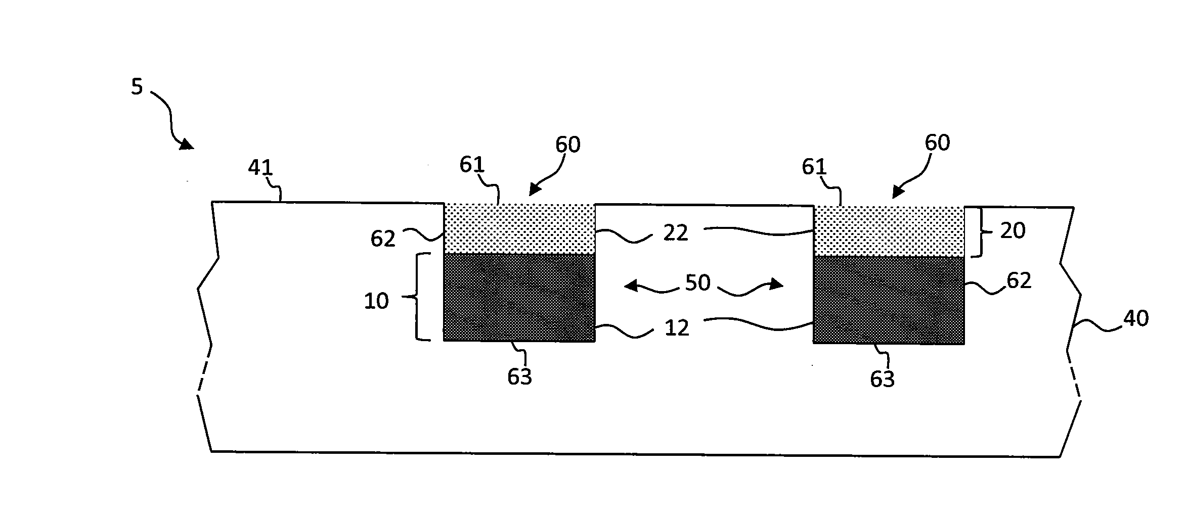
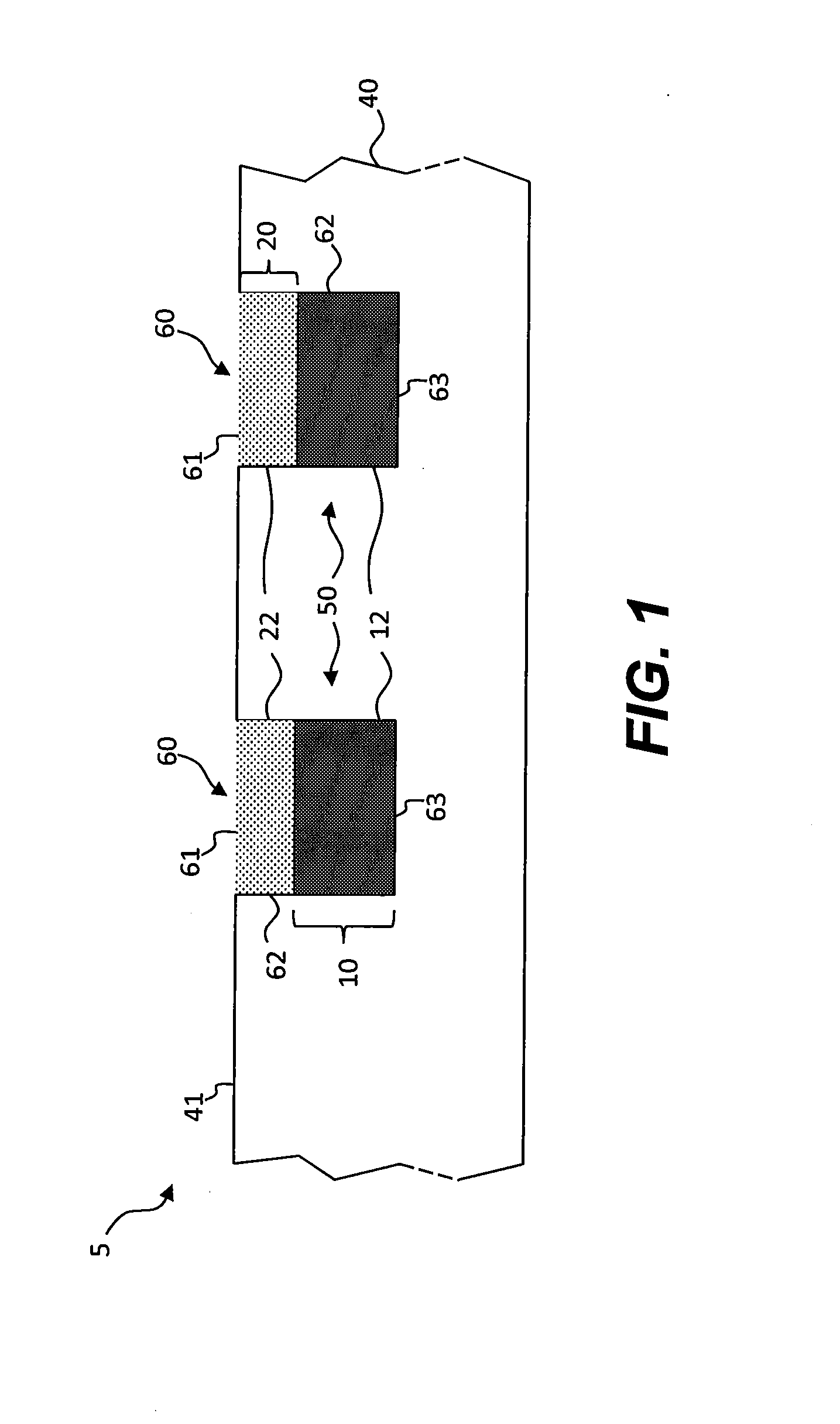
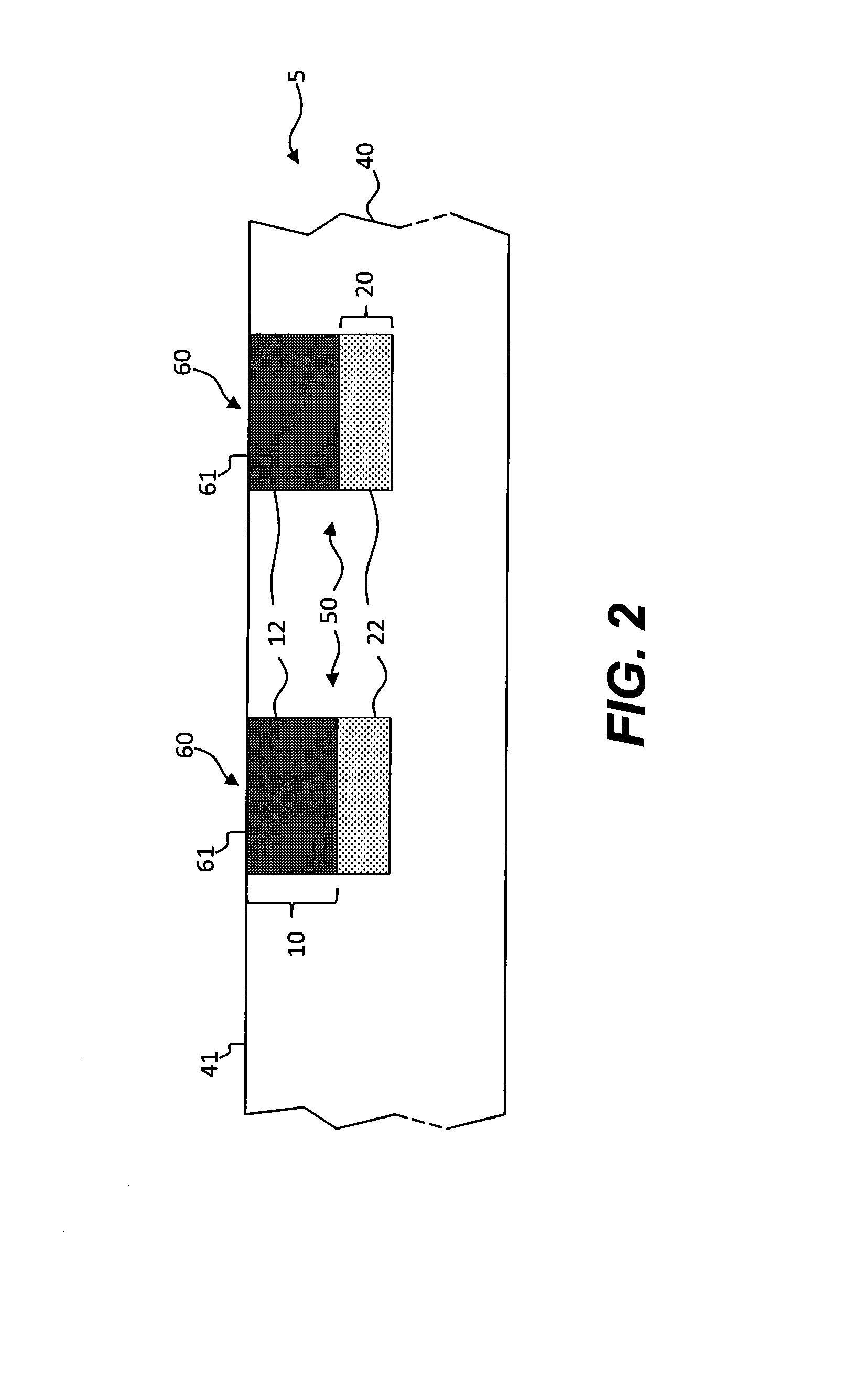
[0031]The present invention is directed toward multi-layer micro-wire structures formed in a substrate that are capable of conducting electrical currents. The electrically conductive multi-layer micro-wire structures provide improved transparency, conductivity, and flexibility, especially in a curved configuration.

[0032]Referring to FIG. 1 in an embodiment of the present invention, a multi-layer micro-wire structure 5 includes a substrate 40 having a substrate surface 41. One or more micro-channels 60 are formed in the substrate 40 and extend into the substrate 40 from the substrate surface 41. The micro-channels 60 have a micro-channel bottom 63, micro-channel sides 62, and a micro-channel top 61. The micro-channel top 61 can be open and correspond to the substrate surface 41. An electrically conductive first material composition 12 forms a first layer 10 located in each micro-channel 60. An electrically conductive second material composition 22 having a greater tensile ductility t...


PUM


Abstract

A multi-layer micro-wire structure resistant to cracking including a substrate having a surface, one or more micro-channels formed in the substrate, an electrically conductive first material composition forming a first layer located in each micro-channel, and an electrically conductive second material composition having a greater tensile ductility than the first material composition forming a second layer located in each micro-channel, the first material composition and the second material composition in electrical contact to form an electrically conductive multi-layer micro-wire in each micro-channel, whereby the multi-layer micro-wire is resistant to cracking

Description

CROSS REFERENCE TO RELATED APPLICATIONS[0001]Reference is made to commonly-assigned U.S. patent application Ser. No. ______ (Docket K001762) filed concurrently herewith, entitled “Making Multi-Layer Micro-Wire Structure” by Spath et al, the disclosure of which is incorporated here.[0002]Reference is made to commonly-assigned U.S. patent application Ser. No. 14 / 032,213, filed Sep. 20, 2013, entitled “Micro-Wire Touchscreen with Unpatterned Conductive Layer” by Burberry et al, and to commonly-assigned U.S. patent application Ser. No. 13 / 779,917, filed Feb. 28, 2013, entitled “Multi-Layer Micro-Wire Structure” by Yau et al, the disclosures of which are incorporated herein.FIELD OF THE INVENTION[0003]The present invention relates to micro-wire electrical conductors.BACKGROUND OF THE INVENTION[0004]Transparent conductors are widely used in the flat-panel display industry to form electrodes for electrically switching the light-emitting or light-transmitting properties of a display pixel, ...

Claims


Application Information

Patent Timeline
IPC IPC(8): H05K1/02G06F3/044H05K1/09G06F3/041
CPCH05K1/0298G06F3/0412H05K2201/09036H05K1/097H05K1/0274G06F3/044H05K3/247H05K2201/0338H05K2201/035H05K2201/0376H05K2203/0108H05K2203/1545H05K3/1258H05K2201/0108H05K2201/0329G06F3/047G06F2203/04103G06F2203/04112H05K1/189
Inventor SPATH, TODD MATHEWCOK, RONALD STEVEN
Owner EASTMAN KODAK CO
Why Eureka
Try Eureka