Quasi TEM dielectric travelling wave scanning array
a scanning array and dielectric technology, applied in the field of coupling, can solve problems such as bandwidth constraints, and achieve the effect of increasing the instantaneous bandwidth of the array
- Summary
- Abstract
- Description
- Claims
- Application Information
AI Technical Summary
Benefits of technology
Problems solved by technology
Method used
Image

Examples
Embodiment Construction
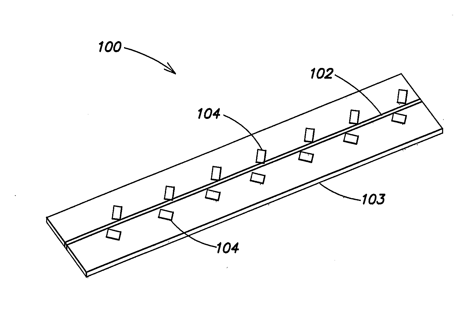
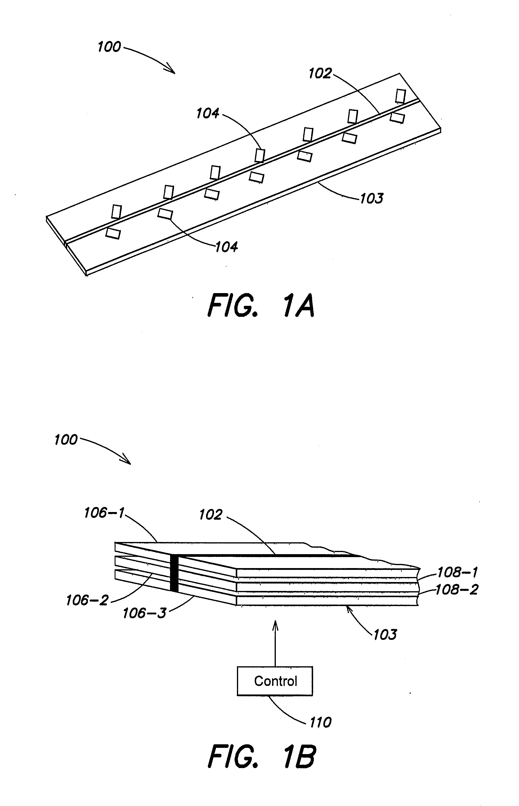
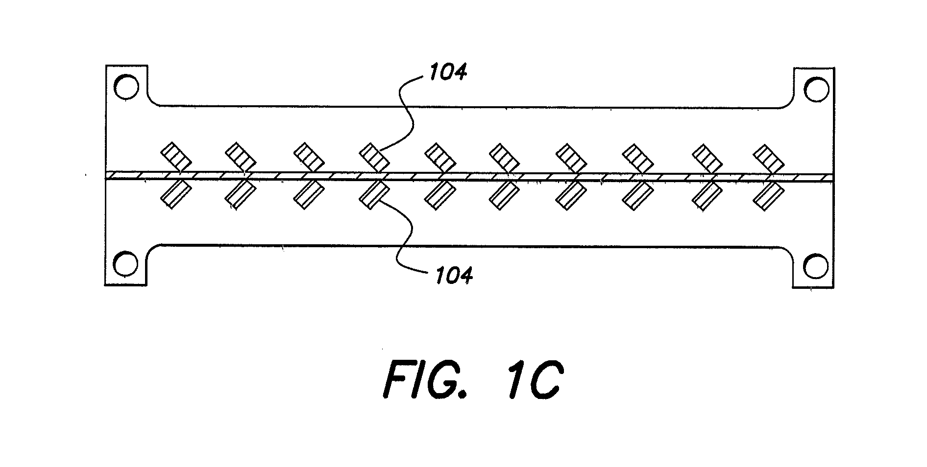
[0027]Antenna array elements are fed in series by a coupling feed structure formed from a Transverse Electromagnetic Mode (TEM) or quasi-TEM transmission line disposed adjacent an adjustable substrate. The adjustable substrate may be formed of two or more dielectric layers, with the dielectric layers having a reconfigurable gap between them. The transmission line may be a low dispersing microstrip, stripline, slotline, coplanar waveguide, or any other quasi-TEM or TEM transmission line structure. The gaps introduced in between the dielectric layers provide variable properties, such as a variable dielectric constant (variable epsilon structure) to control the scanning of the array. Alternatively, a piezoelectric or ElectroActive Polymer (EAP) actuator material may provide or control the gaps between layers, allowing these layers to expand, or causing a gel, air, gas, or other material to compress. Any other arrangement may be used to enable the dielectric constant of the adjacent str...
PUM
 Abstract
Description
Claims
Application Information
 - R&D
- Intellectual Property
- Life Sciences
- Materials
- Tech Scout
- Unparalleled Data Quality
- Higher Quality Content
- 60% Fewer Hallucinations
Browse by: Latest US Patents, China's latest patents, Technical Efficacy Thesaurus, Application Domain, Technology Topic, Popular Technical Reports.
© 2025 PatSnap. All rights reserved.Legal|Privacy policy|Modern Slavery Act Transparency Statement|Sitemap|About US| Contact US: help@patsnap.com