

Method for production of optical waveguides and coupling and devices made from the same
a technology of optical waveguides and couplings, applied in the field of production of highlyconfined optical nanowaveguides, can solve the problems of large optical waveguides which are not suitable for many novel optical circuits, conventional etching methods present significant challenges, and the optical energy to leak or radiate out, etc., to achieve high selectivity, low loss optical waveguides, and high refractive index contrast
- Summary
- Abstract
- Description
- Claims
- Application Information
AI Technical Summary
Benefits of technology
Problems solved by technology
Method used
Image

Examples
Embodiment Construction
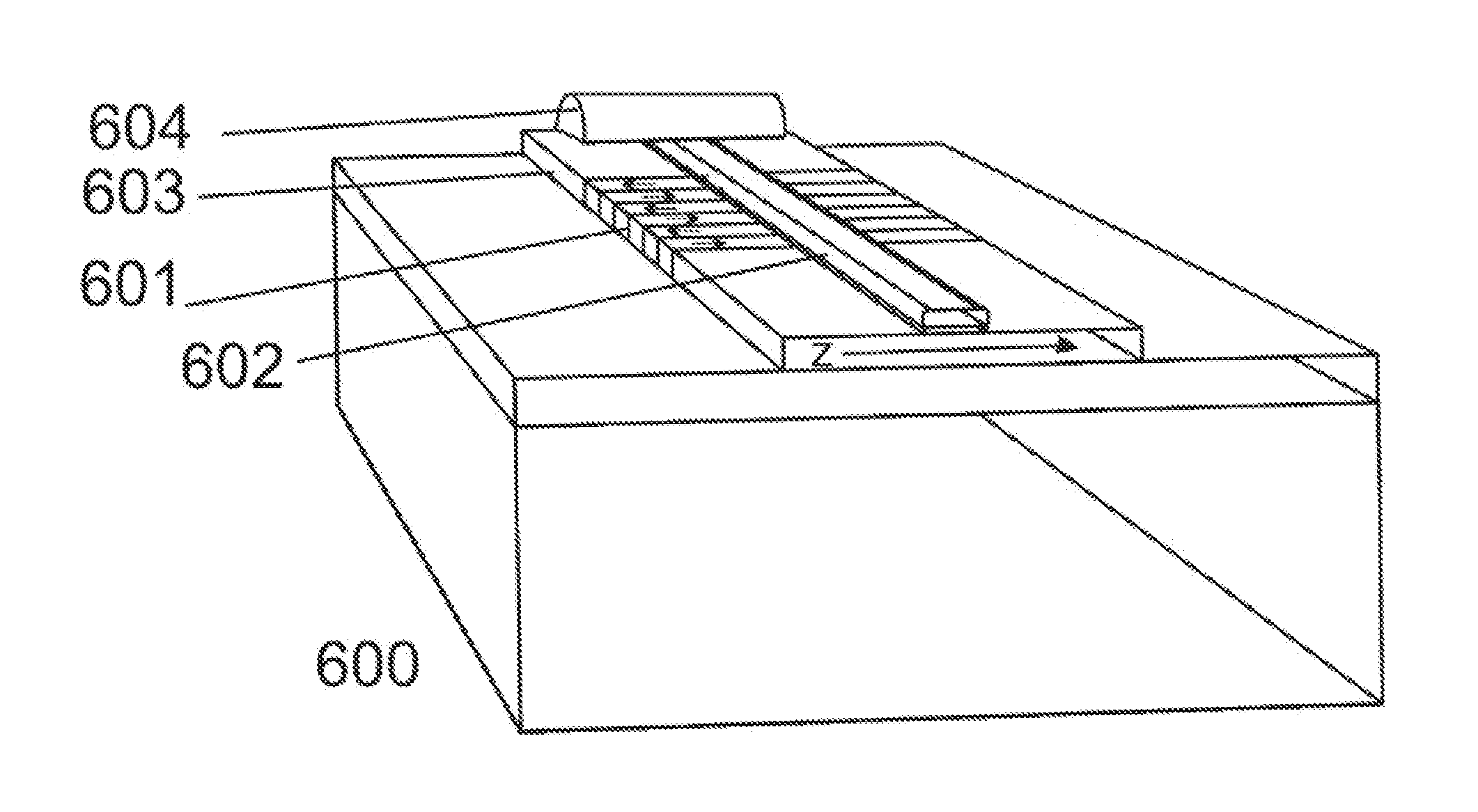
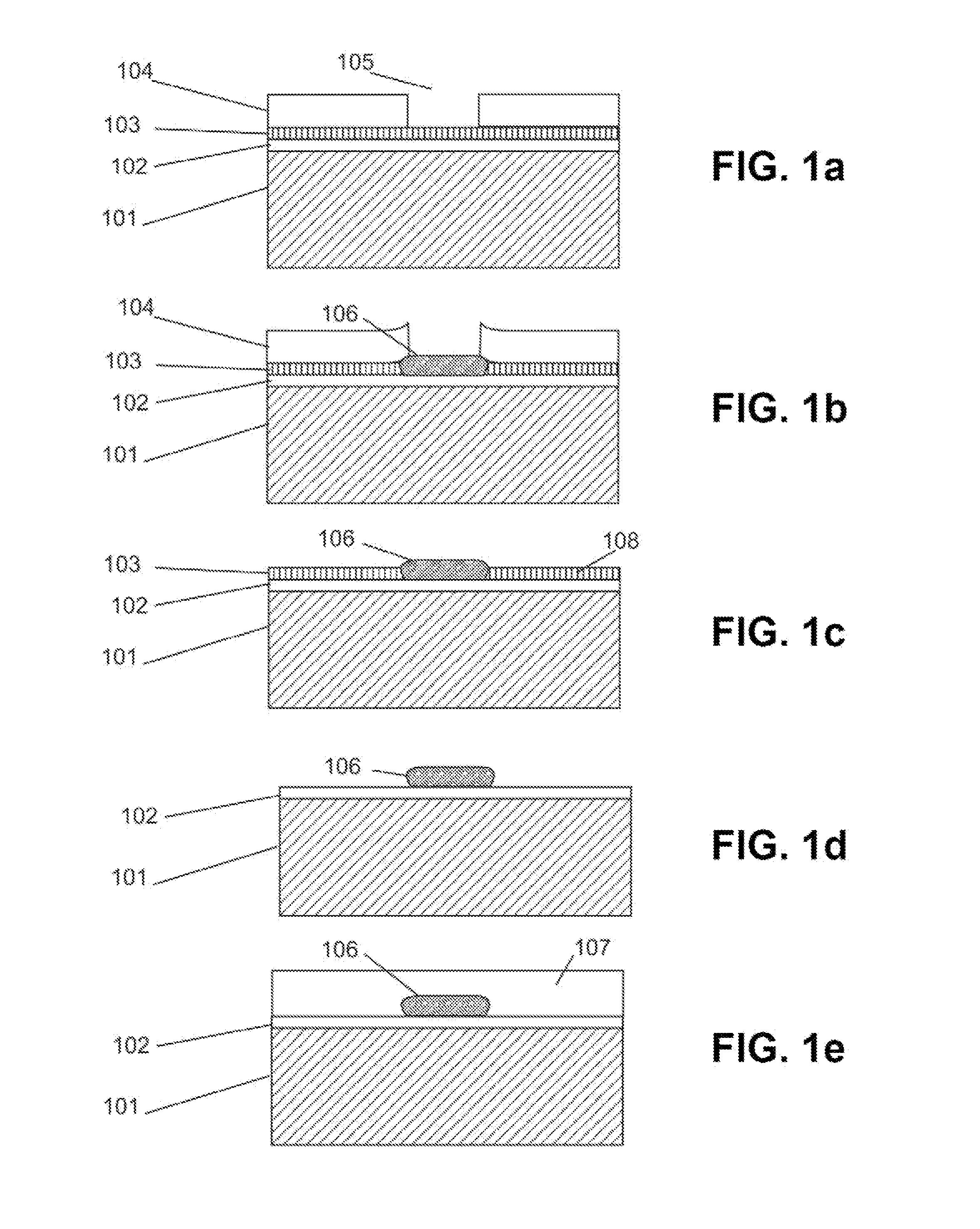
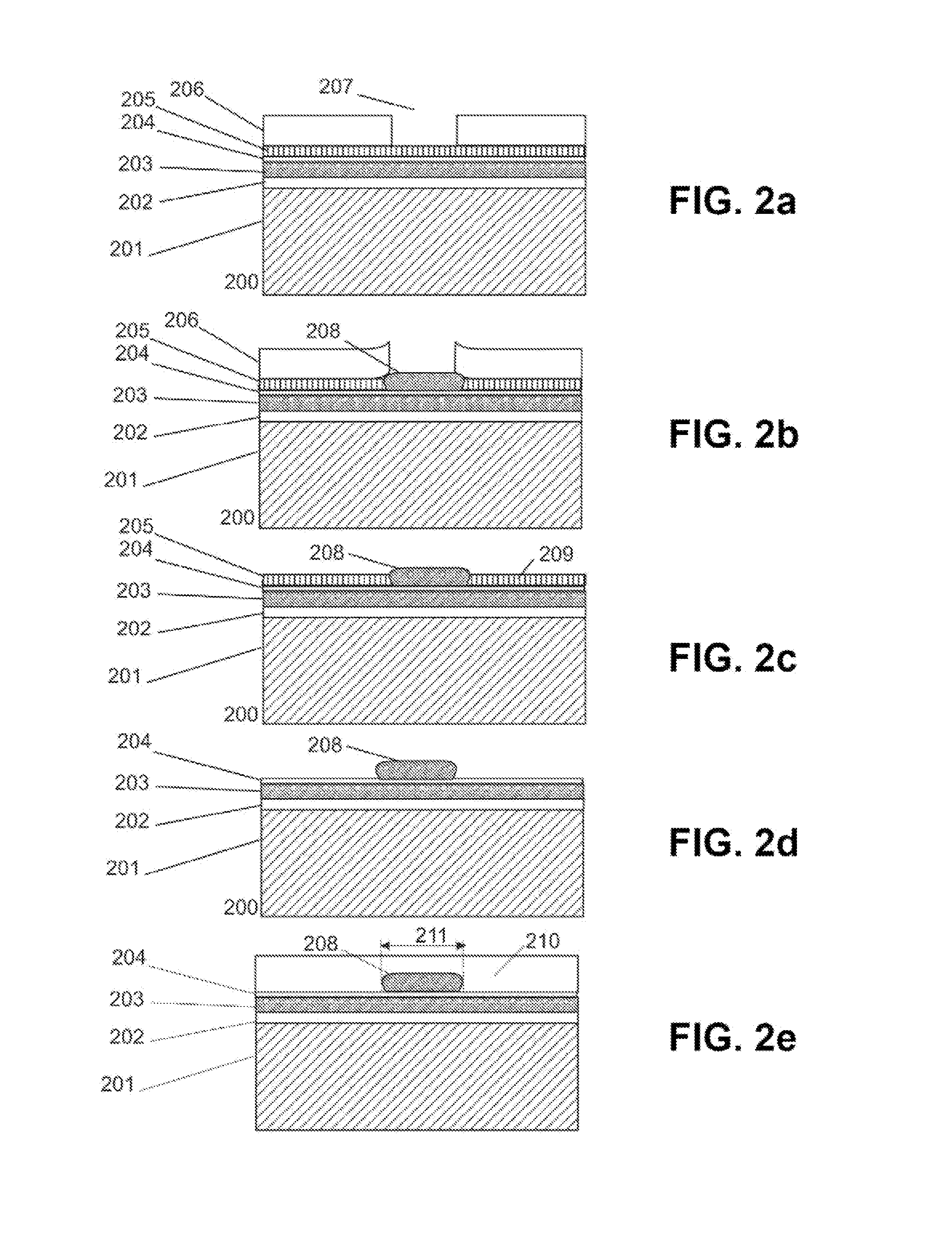
[0040]Specific embodiments of the invention will now be described in detail with reference to the accompanying figures. Like elements in the various figures are denoted by like reference numerals for consistency.
[0041]In the following detailed description of embodiments of the invention, numerous specific details are set forth in order to provide a more thorough understanding of the invention. However, it will be apparent to one of ordinary skill in the art that the invention may be practiced without these specific details. In other instances, well-known features have not been described in detail to avoid unnecessarily complicating the description.
[0042]The detailed description is presented largely in terms of procedures, logic blocks, processing, and / or other symbolic representations that directly or indirectly resemble a novel high-refractive index contrast waveguide, a method of manufacturing a high-refractive index contrast waveguide, and / or a method of low loss and efficient op...
PUM
| Property | Measurement | Unit |
|---|---|---|
| width | aaaaa | aaaaa |
| dimensions | aaaaa | aaaaa |
| radius | aaaaa | aaaaa |
Abstract
Description
Claims
Application Information