

Preparation method of photonic crystal scintillator by using polymer template
A photonic crystal and scintillator technology, applied in the field of nuclear radiation detection, can solve the problems affecting the overall structure stability, adverse light extraction efficiency, reduction of refractive index contrast, etc., achieves favorable light extraction efficiency, easy to prepare large area Structure, low cost effect
- Summary
- Abstract
- Description
- Claims
- Application Information
AI Technical Summary
Problems solved by technology
Method used
Image

Examples
Embodiment 1
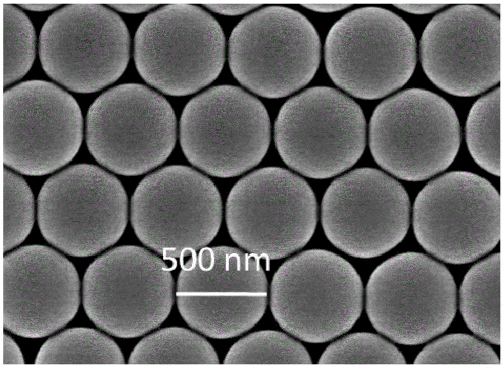
[0033] In this example we will be at (Lu,Y) 2 SiO 5 : Prepare a photonic crystal structure on the surface of Ce scintillator, the scintillator luminescence center wavelength is 420nm, choose polystyrene microspheres with a diameter of 500nm (mass percentage is 2.5%, purchased by Sigma company). (Lu,Y) to be purchased from Sikas 2 SiO 5 : The Ce scintillator is cut and polished into a scintillator substrate with an area of 10mmX10mm and a thickness of 1mm.
[0034] 1. Microsphere array preparation.
[0035] (1) Wafer processing. A 10% sodium dodecyl methyl sulfate solution was prepared, and the silicon wafer was put into the solution for 24 hours.
[0036] (2) Preparation of polystyrene microsphere solution. Take a certain amount of polystyrene microsphere solution and absolute ethanol, and mix them in a ratio of 1:1.
[0037] (3) Drop the prepared polystyrene microsphere solution onto the treated silicon wafer, wait for it to fully unfold on the silicon wafer, and com...
Embodiment 2
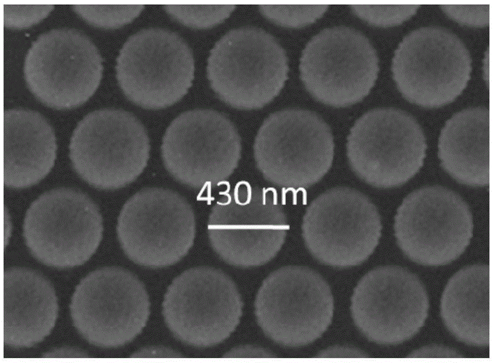
[0044] In this example we will be at Bi 4 Ge 3 o 12 A photonic crystal structure was prepared on the surface of the scintillator. The central wavelength of the scintillator light emission was 520nm, and polymethyl methacrylate microspheres with a diameter of 600nm (2.5% by mass, purchased from Sigma Company) were selected. Bi to be purchased from Sikas 4 Ge 3 o 12 The scintillator is cut and polished into a scintillator substrate with an area of 20mm×20mm and a thickness of 3mm.
[0045] 1. Microsphere array preparation.
[0046] (1) Wafer processing. A 5% sodium dodecyl methyl sulfate solution was prepared, and the silicon wafer was put into the solution for 12 hours.
[0047] (2) Preparation of polymethyl methacrylate microsphere solution. Take a certain amount of polymethyl methacrylate microsphere solution and absolute ethanol, and mix them in a ratio of 1:1.
[0048] (3) Drop the prepared polymethyl methacrylate microsphere solution onto the treated silicon waf...
Embodiment 3
[0055] A kind of method utilizing polymer template to prepare photonic crystal scintillator, adopts following steps:
[0056] (1) Preparation of polymer microsphere array on scintillator surface:
[0057] (1-1) Treating silicon wafers: preparing a sodium dodecyl methylsulfate solution with a concentration of 8 wt%, and placing the silicon wafers in it for 18 hours;
[0058] (1-2) Prepare the polymer microsphere solution: mix the polystyrene microsphere solution with a concentration of 2.5-5wt% and absolute ethanol at a volume ratio of 1:1;
[0059] (1-3) Drop the polymer microsphere solution onto the treated silicon wafer, and wait until it is fully developed on the silicon wafer and the moisture is completely volatilized;
[0060] (1-4) Slowly put the silicon chip dripped with the polymer microsphere solution into the deionized water, the polymer microsphere array will be separated from the silicon chip, and float on the water surface to form a single-layer microsphere array...
PUM
| Property | Measurement | Unit |
|---|---|---|
| Heart wavelength | aaaaa | aaaaa |
| Luminescence center wavelength | aaaaa | aaaaa |
| Diameter | aaaaa | aaaaa |
Abstract
Description
Claims
Application Information