Semiconductor Materials and Devices

a technology of semiconductor materials and materials, applied in the direction of semiconductor devices, lasers, semiconductor lasers, etc., can solve the problem of reducing the likelihood of dislocation in the finished structure, and achieve the effect of good etch selectivity and less damage to other parts of the structur

Inactive Publication Date: 2008-03-20
UNIV OF STRATHCLYDE
View PDF2 Cites 13 Cited by
  • Summary
  • Abstract
  • Description
  • Claims
  • Application Information

AI Technical Summary

Benefits of technology

[0008] The lattice match between the AlxInyGa1-x-yN layer and the at least one further layer in the AlInGaN material system may be such that the in plane strain is less than + / −1%. This reduces the likelihood of dislocations in the finished structure.
[0011] The value of x is preferably chosen such that the strain caused by lattice mismatch to the first gallium rich group III nitride layer is less than + / −0.25% in order to reduce the likelihood of any strain within the device structure.
[0013] The fabrication facilitation layer may provide a differential etch rate between itself and one or both of the adjacent layers composed from the AlInGaN material system. This permits the fabrication facilitation layer to further function as an etch stop layer.
[0029] According to a fourth aspect a method of selectively etching a first gallium rich group III nitride layer from a second gallium rich group III nitride layer, the method comprising growing a AlxInyGa1-x-yN fabrication facilitation layer on a first surface of the first gallium-rich group III nitride layer; growing the second gallium rich group III nitride layer on the fabrication facilitation layer; etching one of the first gallium rich group III nitride layer and the second gallium rich group III nitride layer and terminating the etching process at the fabrication facilitation layer wherein x and y are such as to provide lattice match with at least one of the gallium rich group III nitride layers such that the in plane strain is less than + / −1%. The etching may be terminated in response to detection of chemical species liberated from the fabrication facilitation layer. In other words, the fabrication facilitation layer further provides an etch marking function.
[0031] The fabrication facilitation layer may be further etched away. This may be performed using a wet etching technique such as an alkaline wet etch and is preferably used to provide a flat surface for deposition of the Distributed Bragg Reflector (DBR). The alkaline etch may comprise a high-temperature solvent-free melt, exemplified by a eutectic mixture of sodium hydroxide (NaOH) and potassium hydroxide (KOH) at temperatures above 230° C. Alternatively, the facilitation layer may be etched using an acid based wet etch. An advantage of using an acid based etch is that such etches may cause less damage to other parts of the structure than corresponding alkaline etches. To allow an acid etch to be used, the method may further involve selectively converting areas of the AlxInyGa1-x-yN fabrication facilitation layer exposed by the etching process to an oxide and etching the oxide using an acid based etch. Techniques for forming an oxide on AlxInyGa1-x-yN are described by Dorsaz et al in Applied Physics Letters, Vol 87, 072102, 2005.

Problems solved by technology

This reduces the likelihood of dislocations in the finished structure.

Method used


Image

  • Semiconductor Materials and Devices
  • Semiconductor Materials and Devices
  • Semiconductor Materials and Devices

Examples


first embodiment

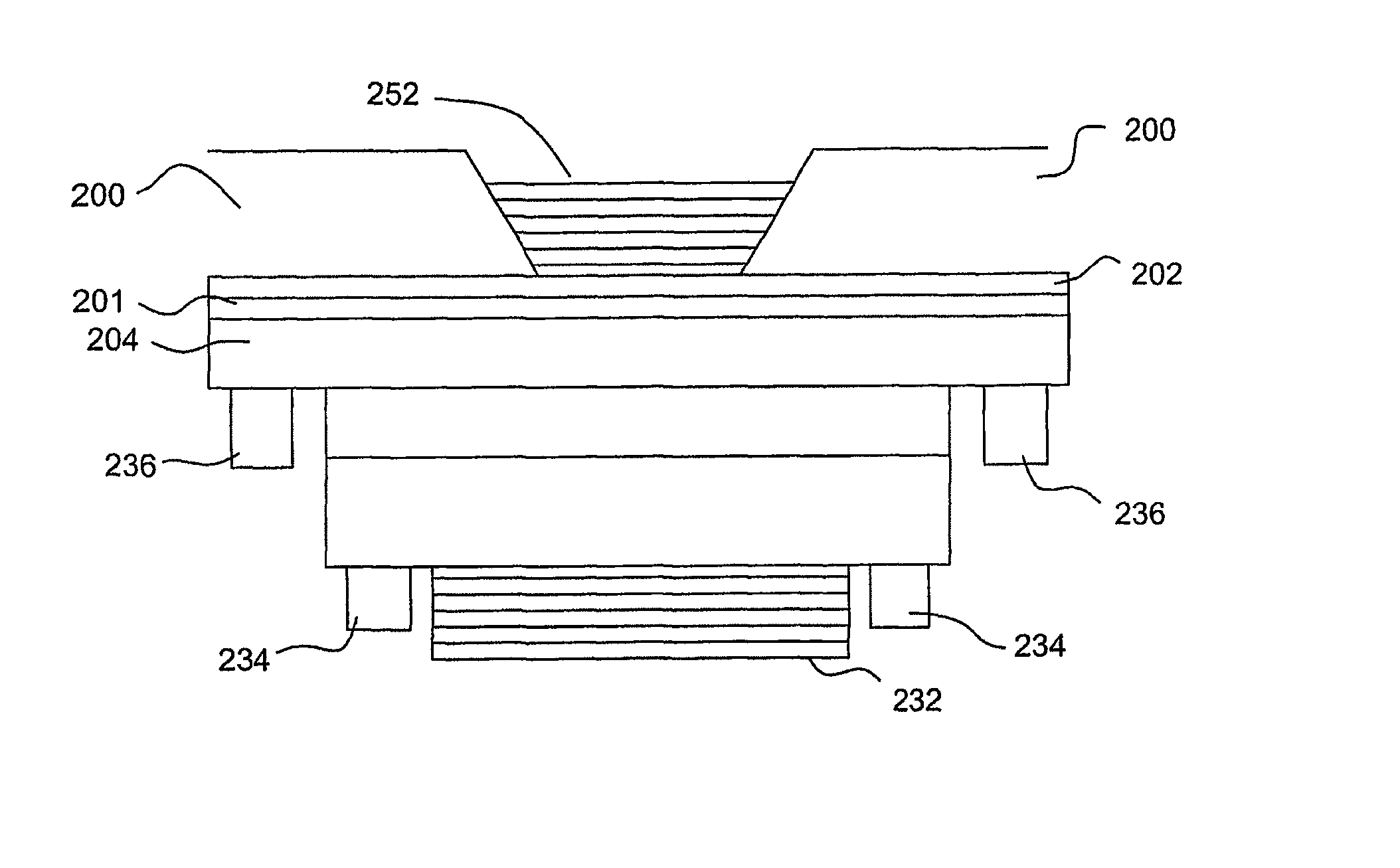
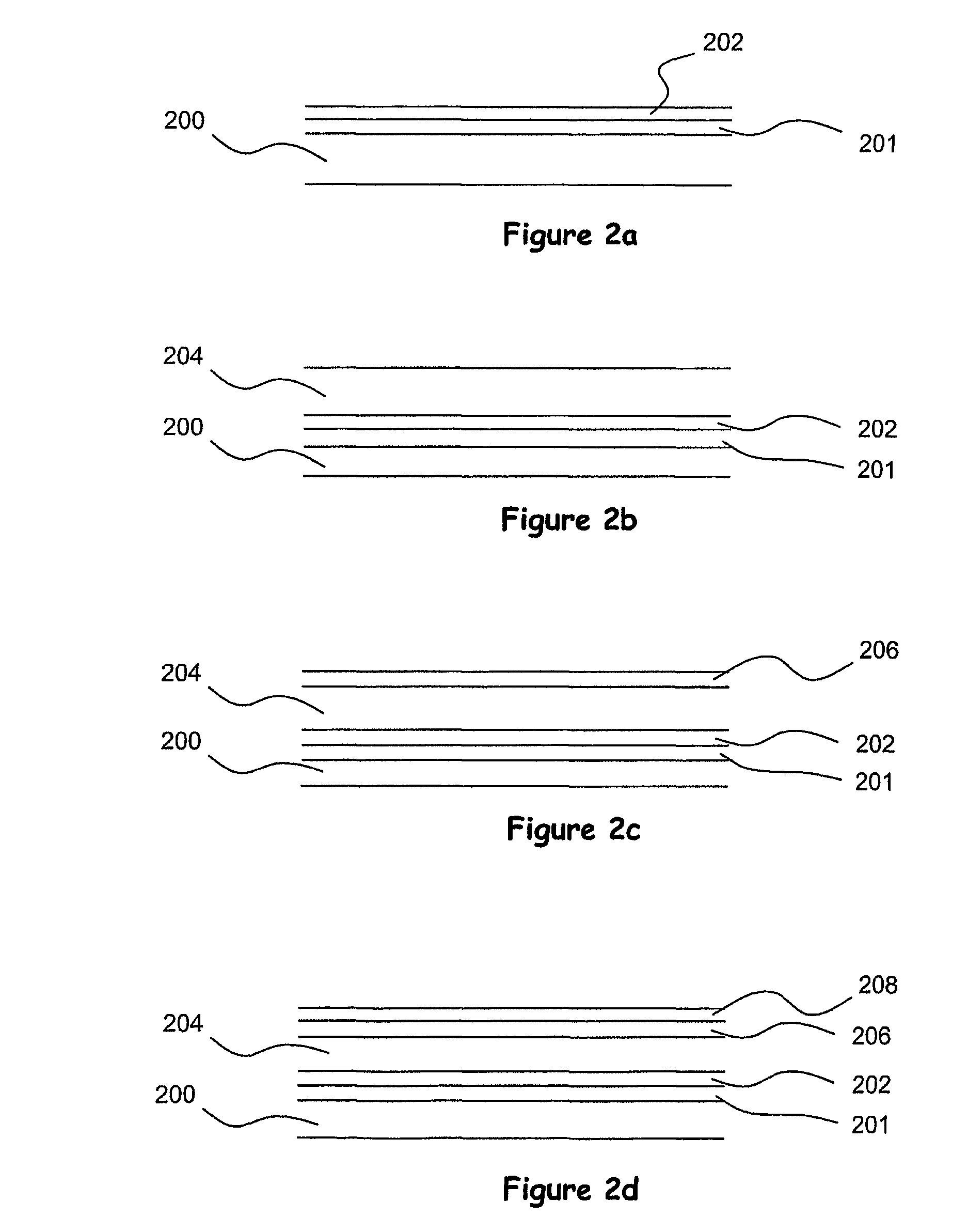
[0046] The growth of a VCSEL device for emission in the violet spectral region according to the invention will now be described. FIG. 2(a) shows a gallium nitride substrate 200, typically 300 μm thick. The substrate typically comprises a lower layer that has been grown comparatively quickly (to provide cost-effective manufacture) and an upper layer that has been grown comparatively slowly (to provide a smooth surface for subsequent growth). Alternatively the lower layer could be a substrate of a different material such as sapphire. In FIG. 2(a) the smooth surface is shown uppermost. On this upper surface is grown a gallium nitride buffer layer 201 that has optical properties that are substantially the same as those of the gallium nitride substrate 200. This has a thickness of 1 micron. As will be appreciated, this layer 201 is optional. On the buffer layer 201 is an Al0.83In0.17N layer 202 that is grown by MOVPE (also known as MOCVD). This provides a very good in-plane lattice match...

second embodiment

[0069] In the examples above, the growth was conducted using MOCVD. However, other growth techniques are possible such as Molecular Beam Epitaxy (MBE). MBE generally has a more predictable (albeit slower) growth rate than MOCVD so it might be possible to grow the active region in a VCSEL using MBE without requiring optical monitoring. However, the use of the growth facilitation layer for either stopping an etch process or detecting when such a process should be stopped would still apply. The modified technique of the second embodiment could also be applied to remove the fabrication facilitation layer using a wet etch.

[0070] A skilled person will appreciate that variations of the disclosed arrangements are possible without departing from the invention. For example, whilst the AlxInyGa1-x-yN fabrication facilitation layer is described as being a single layer, it could be implemented as multiple layers, for example as a superlattice structure. Equally, rather than having a uniform comp...


PUM

PropertyMeasurementUnit
thicknessaaaaaaaaaa
thicknessaaaaaaaaaa
temperaturesaaaaaaaaaa

Abstract

A method of growing semiconductor materials in the Indium, Aluminium, Gallium Nitride (InAlGaN) material system and to devices made therefrom, in particular optical devices in the ultraviolet to green region of the visible spectrum. Certain optical devices, for example Vertical Cavity Surface Emitting Lasers (VCSELs) require great precision in the thickness of certain semiconductor layers. One aspect of the present invention provides a gallium-rich group III nitride layer (200, 201) and an adjacent layer of AlxInyGa1-x-yN layer (202). The AlxInyGa1-x-yN layer (202) acts as a fabrication facilitation layer and is selected to provide a good lattice match and high refractive index contrast with the gallium-rich group III nitride layer (200, 201). The high refractive index contrast permits in-situ optical monitoring. The extra layer (202) can be used as an etch marker or etch stop layer in subsequent processing and may be used in a lift-off process.

Description

[0001] The present invention relates to semiconductor materials in the Indium, Aluminium, Gallium Nitride (InAlGaN) material system. More specifically it relates to techniques for growing semiconductor layers with high accuracy and to devices fabricated by such techniques. BACKGROUND TO THE INVENTION [0002] Optical semiconductor devices in general, and Vertical Cavity Surface Emitting Lasers (VCSELs) in particular, have critical dimensions in their structures. Typically there will be several layers in such devices whose dimensions are related to the wavelength of the light at which they operate and that need to be grown to close tolerances. [0003] In the case of photonic devices operating in the ultraviolet to green spectral region, the use of semiconductor materials in the InAlGaN material system is strongly favoured. Furthermore, high performance is favoured by growth of materials on gallium-rich group III nitride substrates or buffer layers. The shorter wavelengths of the light a...

Claims


Application Information

Patent Timeline
Patent Type & Authority Applications(United States)
IPC IPC(8): H01L21/00H01L21/311H01L33/00H01L33/32H01S5/04H01S5/183H01S5/343
CPCB82Y20/00H01L33/32H01S5/0207H01S5/041H01S2304/04H01S5/18358H01S5/18369H01S5/18383H01S5/34333H01S5/18341
Inventor WATSON, IAN MICHAELDAWSON, MARTINGU, ERDANMARTIN, ROBERT WILLIAMEDWARDS, PAUL ROGER
Owner UNIV OF STRATHCLYDE
Why Eureka
Try Eureka