Low loss, high and low index contrast waveguides in semiconductors

a low-loss, high-index contrast technology, applied in the field of waveguides, can solve problems such as wave propagation loss

Inactive Publication Date: 2011-08-09
LAWRENCE LIVERMORE NAT SECURITY LLC
View PDF13 Cites 11 Cited by
  • Summary
  • Abstract
  • Description
  • Claims
  • Application Information

AI Technical Summary

Benefits of technology

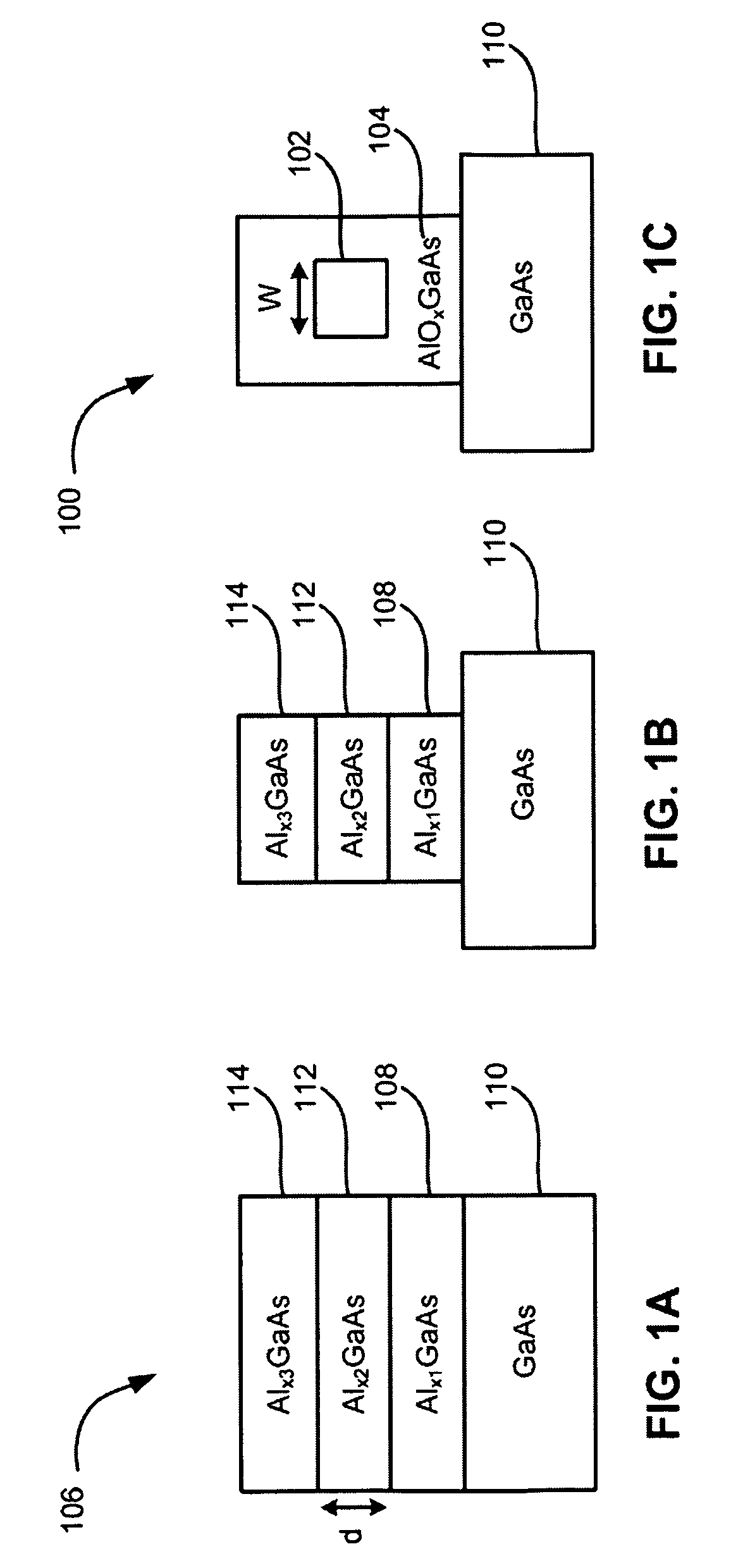
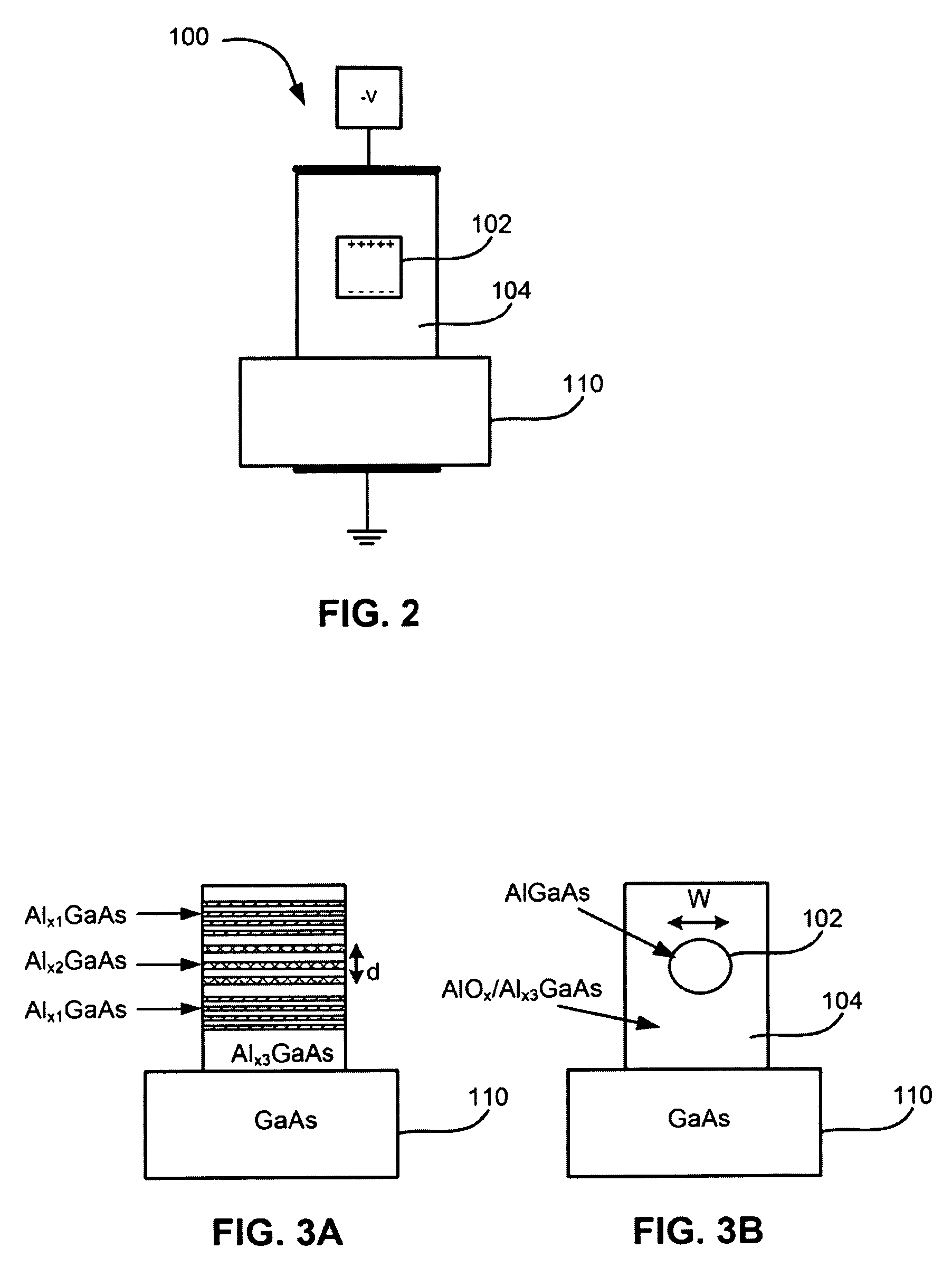
[0006]A system in one general embodiment includes a waveguide structure comprising a core of an alloy of Group III-V materials surrounded by an oxide (which may include one or more Group III-V metals), wherein an interface of the oxide and core is characterized by oxidation of the alloy for defining the core.

Problems solved by technology

Current waveguide technologies exhibit losses on the order of 100-200 dB / m the causes of loss are myriad, and include insertion losses, presence of impurities in the waveguide, bend losses, scattering losses caused by sidewall surface roughness, etc.
For example, the scattering of light from rough sidewall surfaces in semiconductor optical rib waveguides is a primary source of wave propagation loss.
Given the clear fundamental tradeoff between reduced bend size and increased scattering loss, minimizing the sidewall roughness σ becomes perhaps the most critical challenge to achieving a viable photonic integration technology.

Method used


Image

  • Low loss, high and low index contrast waveguides in semiconductors
  • Low loss, high and low index contrast waveguides in semiconductors
  • Low loss, high and low index contrast waveguides in semiconductors

Examples


Embodiment Construction

erface during polishing.

[0024]FIG. 9 shows SEM images of dry-etched Al0.3Ga0.7As ridge structure (a) before oxidation, (b) after 20 min, 450° C. O2-enhanced wet oxidation (7000 ppm O2), and (c) after selective oxide removal in 1:10 BHF:H2O solution for 15 min to reveal oxidation-smoothed interface.

[0025]FIG. 10 shows SEM images of shallow dry-etched Al0.3Ga0.7As ridge structures wet oxidized at 450° C. for 45 min (a) without and (b) with added O2 (7000 ppm), shown after selective oxide removal in 1:10 BHF:H2O for 75 min. The inset shows 500 nm tall ridge structure formed via RIE before oxidation. Image (a) demonstrates the absence of smoothing in the BHF solution.

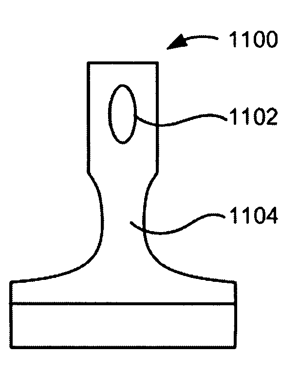
[0026]FIGS. 11A-D illustrate a process for forming a Si-containing waveguide structure according to one embodiment.

[0027]FIGS. 12A-D illustrate a process for forming a Si-containing waveguide structure according to one embodiment.

DETAILED DESCRIPTION

[0028]The following description is made for the purpose of illustrating the...


PUM

PropertyMeasurementUnit
thicknessaaaaaaaaaa
thicknessaaaaaaaaaa
thicknessaaaaaaaaaa

Abstract

A system in one general embodiment includes a waveguide structure comprising a core of an alloy of Group III-V materials surrounded by an oxide (which may include one or more Group III-V metals), wherein an interface of the oxide and core is characterized by oxidation of the alloy for defining the core. A method in one general approach includes oxidizing a waveguide structure comprising an alloy of Group III-V materials for forming a core of the alloy surrounded by an oxide.

Description

RELATED APPLICATIONS[0001]This application claims priority to provisional U.S. application Ser. No. 60 / 932,754 filed on Jun. 1, 2007, which is herein incorporated by reference.[0002]The United States Government has rights in this invention pursuant to Contract No. DE-AC52-07NA27344 between the United States Department of Energy and Lawrence Livermore National Security, LLC for the operation of Lawrence Livermore National Laboratory,FIELD OF THE INVENTION[0003]The present invention relates to waveguides, and more particularly to low loss, high index contrast waveguides in semiconductors.BACKGROUND[0004]Current waveguide technologies exhibit losses on the order of 100-200 dB / m the causes of loss are myriad, and include insertion losses, presence of impurities in the waveguide, bend losses, scattering losses caused by sidewall surface roughness, etc.[0005]For example, the scattering of light from rough sidewall surfaces in semiconductor optical rib waveguides is a primary source of wav...

Claims


Application Information

Patent Timeline
Patent Type & Authority Patents(United States)
IPC IPC(8): G02B6/10
CPCB82Y20/00G02B6/1223G02B6/13H01S5/227H01S5/2004H01S5/204G02B2006/12078
Inventor BOND, TIZIANACOLE, GARRETTGODDARD, LYNFORDKALLMAN, JEFF
Owner LAWRENCE LIVERMORE NAT SECURITY LLC
Why Eureka
Try Eureka