Optical waveguide structure

a waveguide and optical waveguide technology, applied in the field of optical devices, can solve the problems of not being able to achieve the same functionality, and achieve the effects of reducing the coupling of light into the buffer and the cladding layer, reducing the sub-region index, and reducing the out-of-plane divergence of light in the sub-region

Inactive Publication Date: 2007-01-09
QUANTUM NIL LTD +1
View PDF13 Cites 11 Cited by
  • Summary
  • Abstract
  • Description
  • Claims
  • Application Information

AI Technical Summary

Benefits of technology

[0013]The use of an array of sub-regions within a waveguide structure having a refractive index higher than the core layer provides a number of benefits over the prior art. Owing to the high index of the sub-regions the out-of-plane divergence of light in the sub-regions is reduced as compared with the air holes which are typically used in photonic crystal structures. As a result, more light is coupled back into the core material at the rod / core interface. Additionally, as the refractive index of the sub-regions is higher than that of the buffer layer and cladding layers, coupling of light into the buffer and cladding layers is reduced. Thus, the present invention provides greater vertical confinement of light within the waveguide. This fact, coupled with the existence of a photonic bandgap at optical wavelengths, allows tight waveguide bends to be formed with low loss at optical wavelengths. According to the present invention, the core can be made of a material with a refractive index better matched to that of conventional optical fibre, e.g. doped silica or silicon oxynitride. This means that the waveguide can be easily coupled to conventional optical fibres without the need for any additional, complicated coupling structures.
[0014]The nature of the band structure, which arises from using high index sub-regions, is such that the dimensions required for the lattice pitch to produce a bandgap at the wavelength typically used for telecommunications can be much larger than in conventional photonic crystals. As a result, fabrication tolerances are greatly reduced, as the sub-regions can be spaced further apart and each sub-region can be larger. This means that the waveguide of the present invention can be easily fabricated using conventional lithography. Typically, prior photonic crystal fabrication techniques require much higher precision lithography, such as e-beam lithography.

Problems solved by technology

Written grating structures do not interact with light in the same way as photonic crystals and so cannot be used to achieve the same functionality.

Method used


Image

  • Optical waveguide structure
  • Optical waveguide structure
  • Optical waveguide structure

Examples


Embodiment Construction

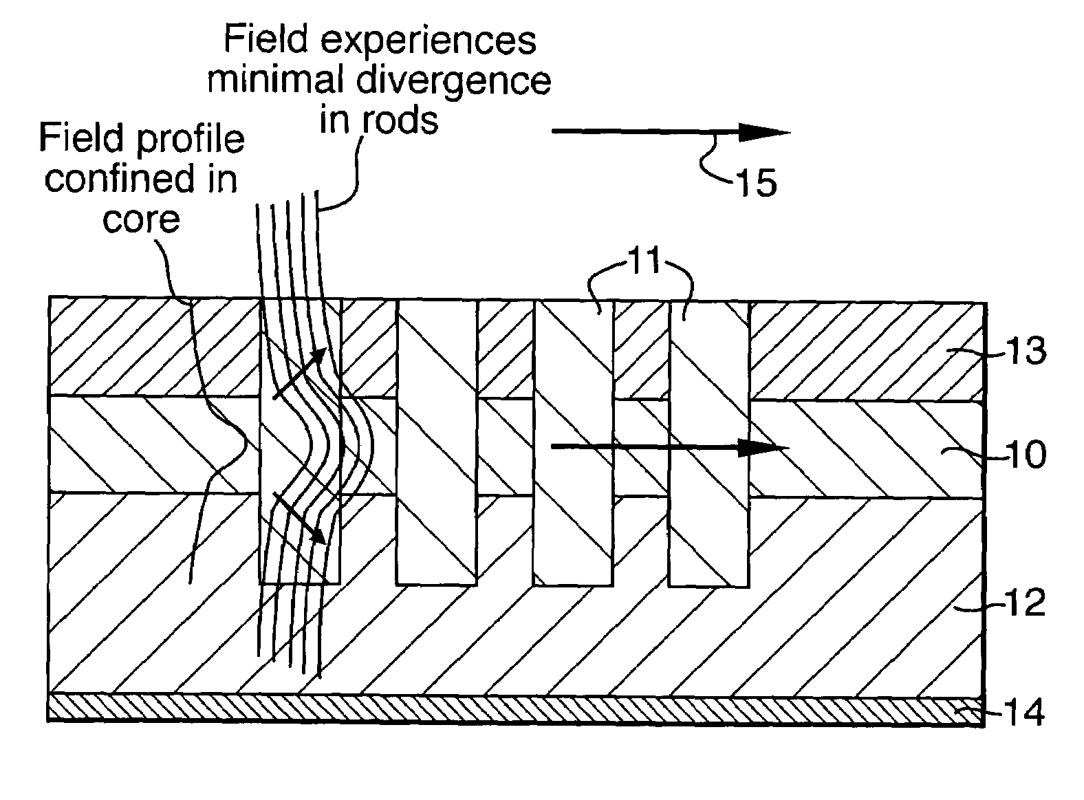
[0052]Photonic crystal waveguide structures are based on some perturbation in dielectric constant in the core of a planar waveguide structure. This has most commonly been performed by the etching of air rods into the core layer of the waveguide. As light propagates through the core it interacts with the dielectric constant modulation and, in some structures, in a manner analogous to electrons in a semiconductor, certain electromagnetic fields are forbidden to propagate in the core. The forbidden electromagnetic fields form a photonic bandgap. More detail on the nature of the band structure of photonic crystals of this sort can be found in WO98 / 53351.

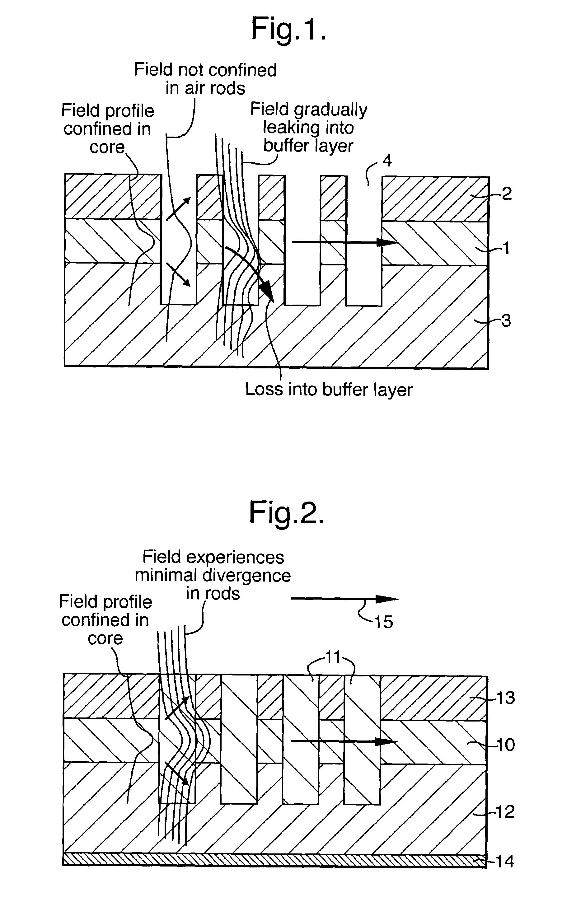
[0053]FIG. 1 illustrates the interaction of the E-field with the core 1 in a photonic crystal according to the prior art. The light is travelling through the core 1 from left to right. A profile of the E-field within the core 1, cladding 2 and buffer 3 layers is shown. It can be seen that in the photonic crystal region the mode confineme...


PUM


Abstract

A waveguide structure according to the invention comprises a core layer (10), having a refractive index ncore, and an array of rods (11) in the core layer having a refractive index nrods. The refractive indices satisfy the inequality: nrods>ncore. In a planar waveguide structure buffer (12) and cladding (13) layers are included, having a refractive index nbuffer and ncladding respectively. The refractive indices then satisfy the inequality: nrods>ncore>ncladding and nbuffer. This condition provides greater vertical confinement of the E-field of an optical signal passing through the waveguide. Furthermore, it allows waveguides to be formed of a glassy material having a similar refractive index and core dimensions to that of a fiber. A high refractive index contrast within the photonic crystal region is used while totally eliminating the need for mode conversion to launch light in and out of the waveguide.

Description

[0001]This application is a continuation-in-part of application Ser. No. 10 / 196,727, filed Jul. 17, 2002 now abandoned.FIELD OF THE INVENTION[0002]The present invention relates to the field of optical devices and in particular but not exclusively to waveguide structures in integrated optical circuits.BACKGROUND TO THE INVENTION[0003]It is increasingly recognised that integrated optical circuits have a number of advantages over electrical circuits. However, it has been difficult to produce integrated optical circuits which are comparably small, primarily due to the difficulty in producing waveguides which can include tight bends without large signal losses. It has also been difficult to produce integrated optical circuits including signal processing devices which can be easily coupled to current optical fibres, owing to a difference in the refractive index of the material used for optical fibres and those materials typically used for integrated optical devices, whilst still maintaini...

Claims


Application Information

Patent Timeline
Patent Type & Authority Patents(United States)
IPC IPC(8): G02B6/10G02B6/122
CPCB82Y20/00G02B6/1225G02B6/02309
Inventor PARKER, GREGCHARLTON, MARTINZOOROB, MAJD
Owner QUANTUM NIL LTD
Why Eureka
Try Eureka