Semiconductor memory device, semiconductor system and reading method

a memory device and semiconductor technology, applied in the field of semiconductor memory devices, can solve the problems of insufficient protection, inability of the memory system to operate normally, increased risk of information leakage, etc., and achieve the effect of improving the security level of specific data

Active Publication Date: 2015-11-12
WINBOND ELECTRONICS CORP
View PDF8 Cites 8 Cited by
  • Summary
  • Abstract
  • Description
  • Claims
  • Application Information

AI Technical Summary

Benefits of technology

[0016]According to the invention, the specific data is read and the specific address information is erased or set to be invalid when the input address information ...

Problems solved by technology

If the security code cannot be read, the memory system is unable to operate normally.
However, storing in advance the information with a high security level in the flash memory and reading the information during an operation renders the following issues.
The risk of information leakage increases if important information such as security code or private information is read mu...

Method used


Image

  • Semiconductor memory device, semiconductor system and reading method
  • Semiconductor memory device, semiconductor system and reading method
  • Semiconductor memory device, semiconductor system and reading method

Examples


Embodiment Construction

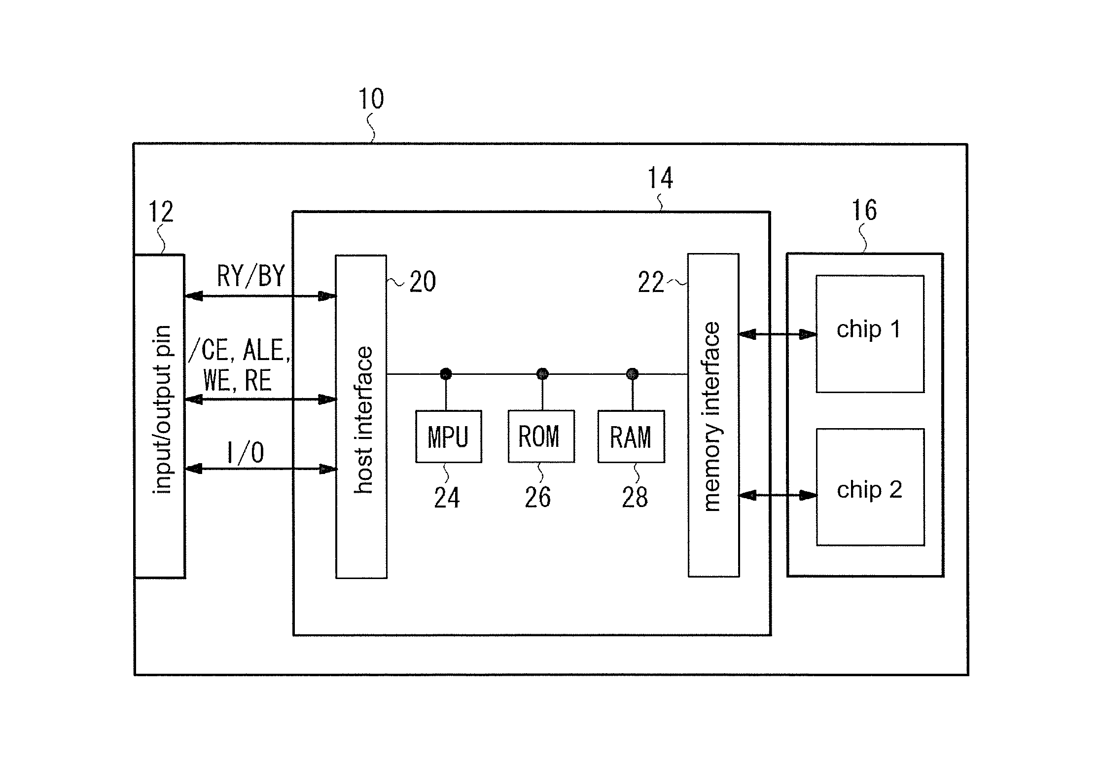
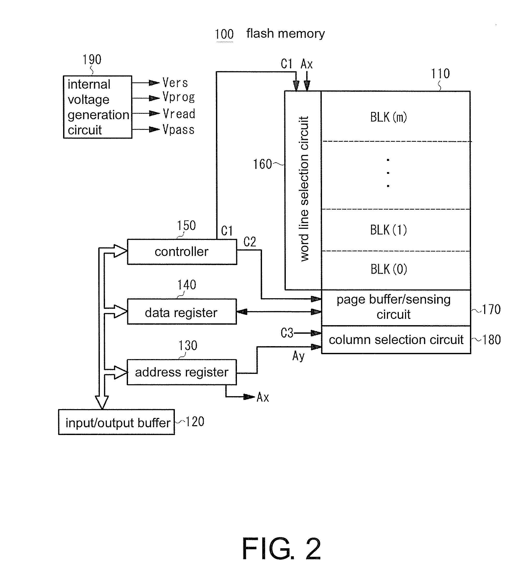
[0032]In the following, the embodiments of the invention are described in detail with reference to the accompanying drawings. FIG. 2 is a diagram illustrating a configuration of a flash memory according to an embodiment of the invention. However, the configuration of the flash memory illustrated herein only serves as an illustrative example. The invention is not limited to the configuration illustrated herein.

[0033]As shown in FIG. 2, a flash memory 100 of this embodiment is configured to include a memory array 110 formed with a plurality of memory cells arranged in an array, an input / output buffer 120 connected to an external input output terminal I / O and keeping input and output data, an address register 130 receiving an address data from the input / output buffer 120, a data register 140 keeping the input and output data, and a controller 150 providing control signals C1, C2, C3, etc., to the respective parts based on command data from the input / output buffer 120 and an external co...


PUM


Abstract

The invention provides a flash memory which may effectively protect information with a high security level. A flash memory includes a setting part. When the setting part is inputted a specific command, the setting part sets up specific address information to a nonvolatile configuration register, and sets up specific data in a hidden storage region. The flash memory also includes: a comparing part, which compares inputted address information and the specific address information during a reading operation; and a control part, which reads specific data set in the storage region and erases a specific address when two address information are consistent, and reads data stored in a memory array according to the inputted address information when two address information are inconsistent.

Description

CROSS-REFERENCE TO RELATED APPLICATION[0001]This application claims the priority benefit of Japan application serial no. 2014-096667, filed on May 8, 2014. The entirety of the above-mentioned patent application is hereby incorporated by reference herein and made a part of this specification.BACKGROUND OF THE INVENTION[0002]1. Field of the Invention[0003]The invention relates to a semiconductor memory device such as a Not AND (NAND) flash memory, and particularly relates to storing and reading of information with a high security level.[0004]2. Description of Related Art[0005]A NAND flash memory has a memory cell array, and the memory cell array includes a NAND string serially connecting a plurality of memory cells. Compared with a NOT OR (NOR) flash memory, the NAND flash memory is capable of realizing a memory cell array having a high density, and is thus suitable for data storage with a large capacity for image or music data. In addition to such purpose, the NAND flash memory also ...

Claims


Application Information

Patent Timeline
IPC IPC(8): G06F3/06
CPCG06F3/061G06F3/0652G06F3/0655G06F3/0688G06F21/575G06F21/79G06F2221/2135G11C16/08G11C16/22G11C16/26G06F21/60G06F9/00
Inventor KAMINAGA, TAKEHIRO
Owner WINBOND ELECTRONICS CORP
Why Eureka
Try Eureka