Chip manufacturing method

a technology of manufacturing method and chip, applied in the direction of glass reforming apparatus, glass making apparatus, manufacturing tools, etc., can solve problems such as productivity reduction

Active Publication Date: 2015-12-03
DISCO CORP
View PDF24 Cites 230 Cited by
  • Summary
  • Abstract
  • Description
  • Claims
  • Application Information

AI Technical Summary

Benefits of technology

[0010]As described above, the chip manufacturing method of the present invention includes the shield tunnel forming step of applying a pulsed laser beam having a transmission wavelength to the platelike workpiece from the focusing means included in the pulsed laser beam applying means along the contour of the chip to be formed in the condition where the focal point of the pulsed laser beam is set at a predetermined depth from the upper surface of the platelike workpiece, thereby forming a plurality of shield tunnels inside the platelike workpiece along the contour of the chip to be formed, each shield tunnel being composed of a fine hole and an amorphous region formed around the fine hole for shielding the fine hole, and the chip forming step of applying ultrasonic vibration to the platelike workpiece processed by the shield tunnel forming step to thereby break the contour of the chip where the shield tunnels have been formed, thereby forming the chip from the platelike workpiece. Accordingly, a chip having a desired shape can be formed in a short time by the chip manufacturing method of the present invention as compared with the conventional chip manufacturing method.

Problems solved by technology

However, there is a problem such that much time is required for etching to cause a reduction in productivity.

Method used


Image

  • Chip manufacturing method
  • Chip manufacturing method
  • Chip manufacturing method

Examples


example 1-1

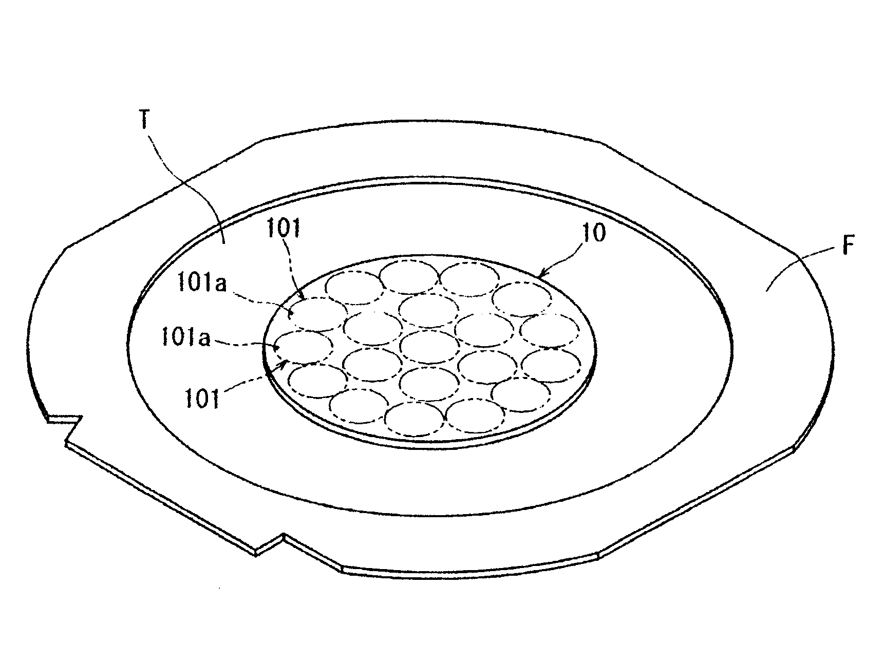
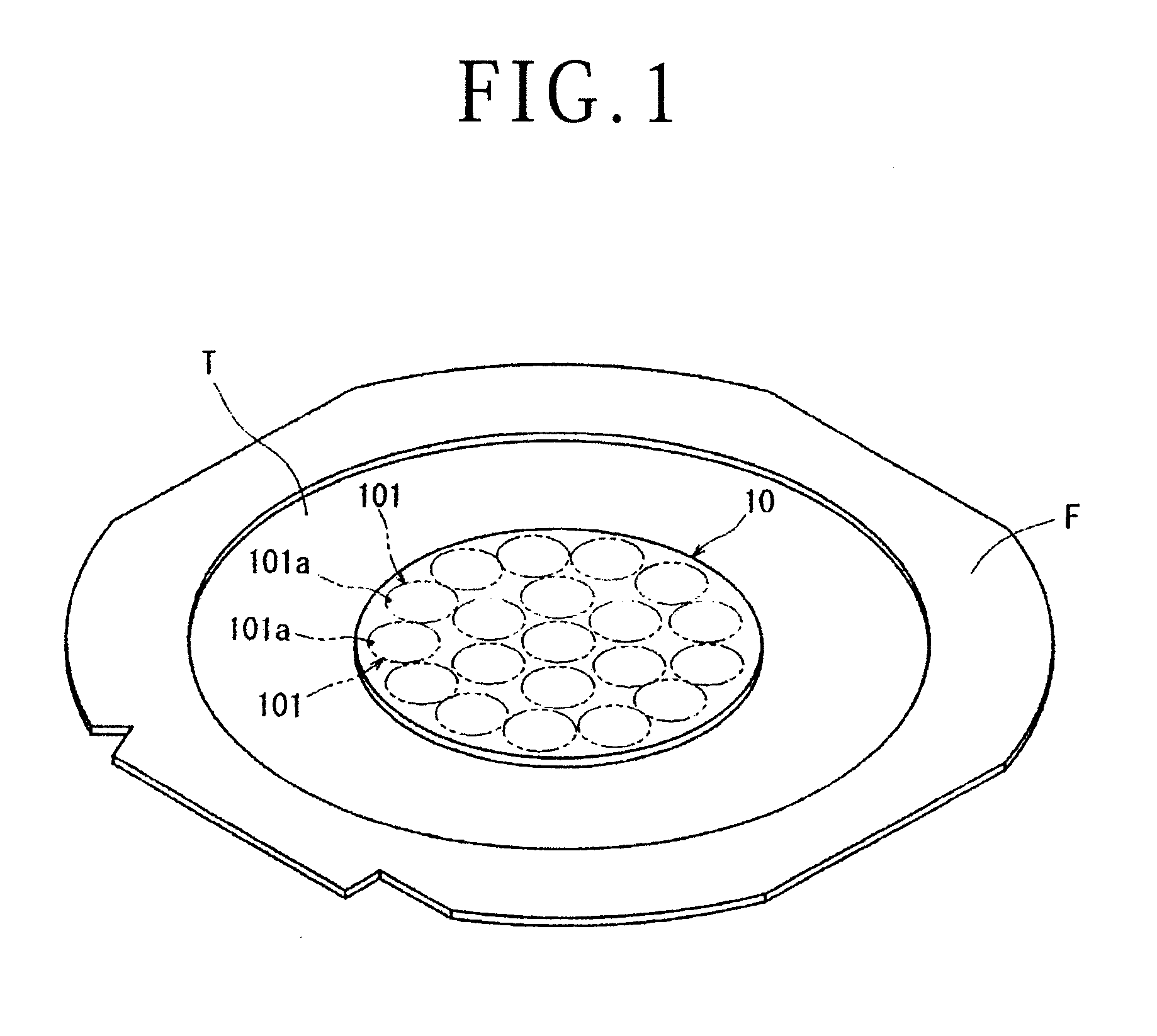
[0039]By using a silica glass substrate (refractive index: 1.45) having a thickness of 500 μm as the platelike workpiece 10, the shield tunnel forming step was performed under the following processing conditions to form a shield tunnel, and it was determined whether or not the shield tunnel is good.

Processing Conditions

[0040]Wavelength: 1064 nm

[0041]Repetition frequency: 50 kHz

[0042]Pulse width: 10 ps

[0043]Average power: 2 W

[0044]Focused spot diameter: 10 μm

[0045]Work feed speed: 500 mm / second

Numerical aperture (NA)Good / poor condition ofof the focusing lensthe shield tunnelS = NA / N0.05Poor: not formed0.0350.1Good0.0690.15Good0.1030.2Good0.1380.25Good0.1720.3Slightly good0.2070.35Poor: voids generated0.2410.4Poor: voids generated0.276

[0046]It is apparent from the above results that in the case of using a silica glass substrate (refractive index: 1.45) as the single crystal substrate a good shield tunnel can be formed by setting the numerical aperture (NA) of the focusing lens 511 for...

example 1-2

[0048]By using a sapphire (Al2O3) substrate (refractive index: 1.76) having a thickness of 500 μm as the platelike workpiece 10, the shield tunnel forming step was performed under the following processing conditions to form a shield tunnel, and it was determined whether or not the shield tunnel is good.

Processing Conditions

[0049]Wavelength: 1064 nm

[0050]Repetition frequency: 50 kHz

[0051]Pulse width: 10 ps

[0052]Average power: 2 W

[0053]Focused spot diameter: 10 μm

[0054]Work feed speed: 500 mm / second

Numerical aperture (NA)Good / poor condition ofof the focusing lensthe shield tunnelS = NA / N0.05Poor: not formed0.1Slightly good0.0570.15Good0.0850.2Good0.1140.25Good0.1420.3Good0.1700.35Good0.1980.4Poor0.2270.45Poor: voids generated0.5Poor: voids generated0.55Poor: voids generated0.6Poor: voids generated

[0055]It is apparent from the above results that in the case of using a sapphire substrate (refractive index: 1.76) as the single crystal substrate a substantially good shield tunnel can be f...


PUM

PropertyMeasurementUnit
refractive indexaaaaaaaaaa
thicknessaaaaaaaaaa
distanceaaaaaaaaaa

Abstract

A chip having a desired shape is formed from a platelike workpiece. The chip manufacturing method includes a shield tunnel forming step of applying a pulsed laser beam to the workpiece from a focusing unit included in a pulsed laser beam applying unit along the contour of the chip to be formed, with the focal point of the pulsed laser beam set at a predetermined depth from the upper surface of the workpiece, thereby forming a plurality of shield tunnels inside the workpiece along the contour of the chip to be formed. Each shield tunnel has a fine hole and an amorphous region formed around the fine hole for shielding the fine hole. In a chip forming step, ultrasonic vibration is applied to the workpiece to break the contour of the chip where the shield tunnels have been formed, thereby forming the chip from the workpiece.

Description

BACKGROUND OF THE INVENTION[0001]1. Field of the Invention[0002]The present invention relates to a chip manufacturing method of forming a chip having a desired shape from a platelike or plate-shaped workpiece such as a glass substrate.[0003]2. Description of the Related Art[0004]An operation screen in a smartphone or the like is formed from a glass substrate, and an operator can select various applications as viewing the operation screen. Further, portable equipment such as a smartphone includes a camera function, and a cover glass such as a silica glass substrate and a sapphire substrate is mounted on an objective lens in the camera function. Such a cover glass or the like is produced in the form of a chip by etching (see Japanese Patent Laid-open Nos. 2012-148955 and 2013-71854, for example).SUMMARY OF THE INVENTION[0005]However, there is a problem such that much time is required for etching to cause a reduction in productivity.[0006]It is therefore an object of the present invent...

Claims


Application Information

Patent Timeline
Patent Type & Authority Applications(United States)
IPC IPC(8): B23K26/00C03B33/08C03B33/02
CPCB23K26/0039B23K26/006C03B33/082C03B33/0222B23K26/0648C03B33/03C03B33/033C03B33/04C03B33/091Y02P40/57B23K26/55
Inventor MORIKAZU, HIROSHITAKEDA, NOBORU
Owner DISCO CORP
Why Eureka
Try Eureka