
Structure and method for integrated circuits packaging with increased density

a technology of integrated circuits and packaging layers, applied in the direction of electrical equipment, semiconductor devices, semiconductor/solid-state device details, etc., can solve the problems of increased complexity of semiconductor manufacturing process, heat dissipation, and stacked dies which utilize tsvs, so as to increase the thermal conductivity of the encapsulation layer and increase the thermal conductivity

Active Publication Date: 2015-12-03
INVENSAS CORP
View PDF11 Cites 62 Cited by
  • Summary
  • Abstract
  • Description
  • Claims
  • Application Information

AI Technical Summary

Benefits of technology

The patent text describes a semiconductor package that includes a substrate with vias and a microelectronic element attached to the substrate. An encapsulation layer made of carbon material is used to improve heat conduction. Another embodiment of the semiconductor package includes a second microelectronic element attached to the substrate and connecting elements made of carbon, which also improve thermal conductivity. Overall, the technical effect of the patent text is to improve the heat transfer and cooling of the semiconductor package.

Problems solved by technology

However, such scaling has also introduced increased complexity to the semiconductor manufacturing process.
However, stacked die which utilize TSVs also present challenges such as heat dissipation, interconnect routing and cell placement, and transistor reliability, among others.

Method used


Image

  • Structure and method for integrated circuits packaging with increased density
  • Structure and method for integrated circuits packaging with increased density
  • Structure and method for integrated circuits packaging with increased density

Examples


Embodiment Construction

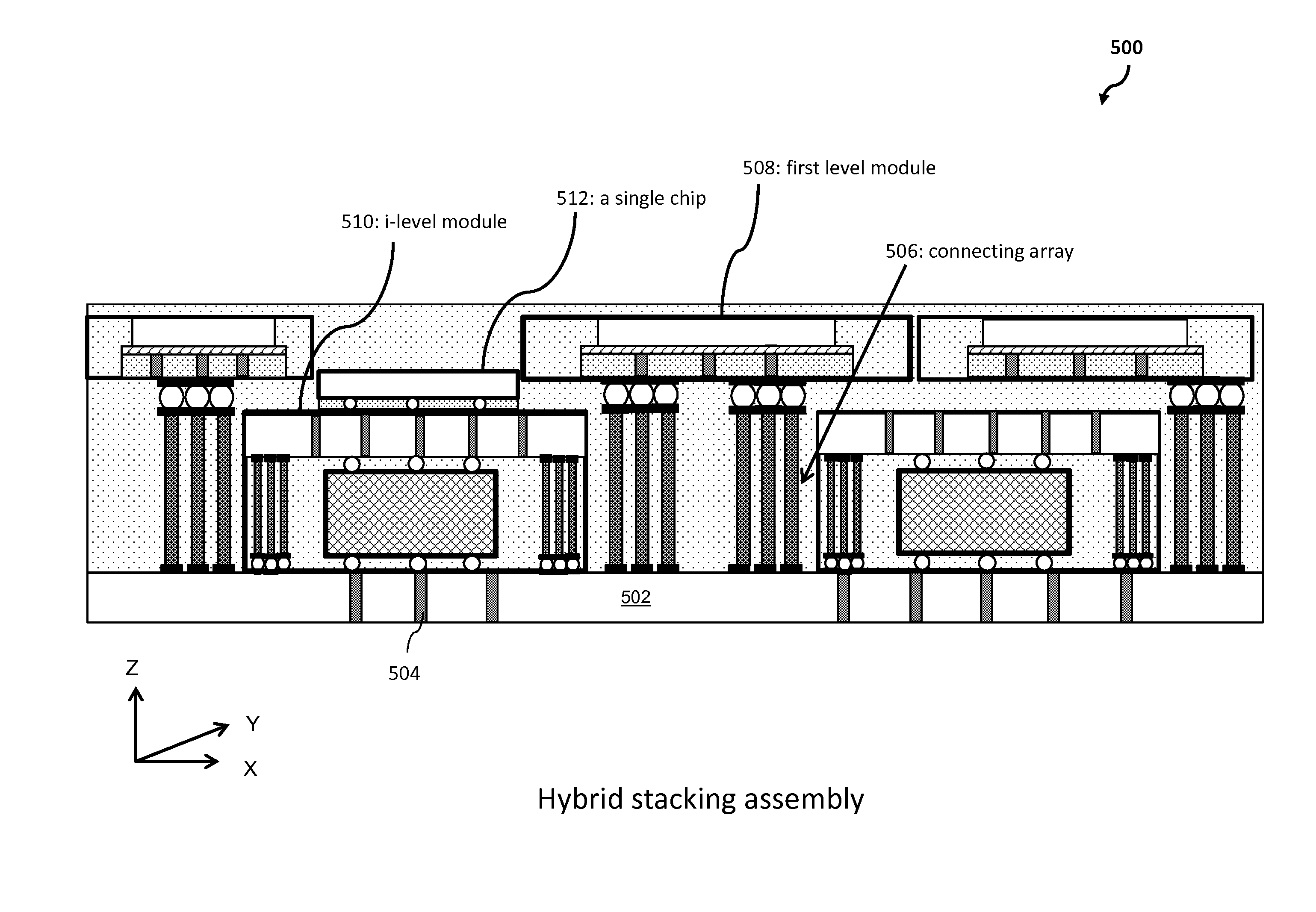
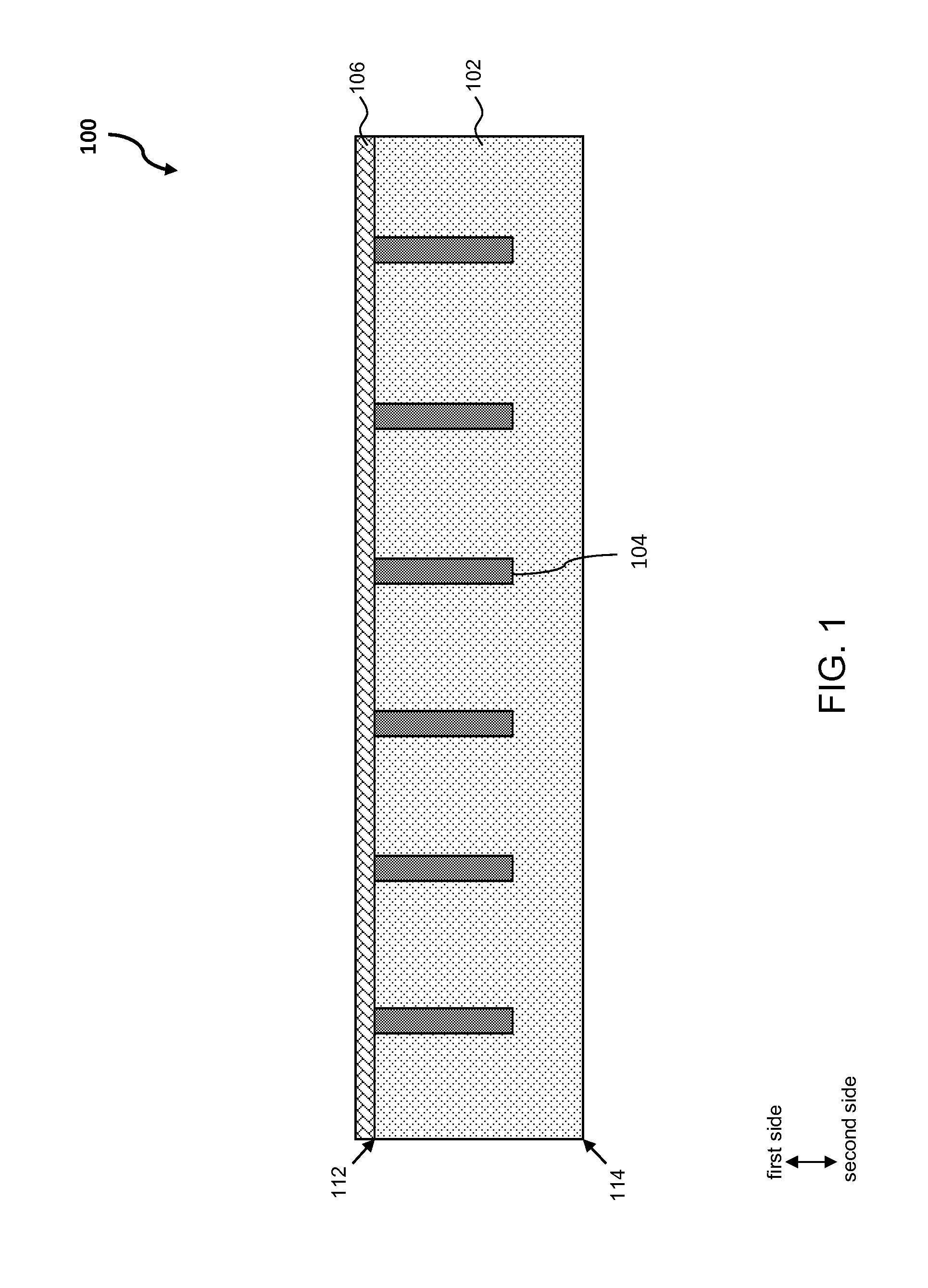
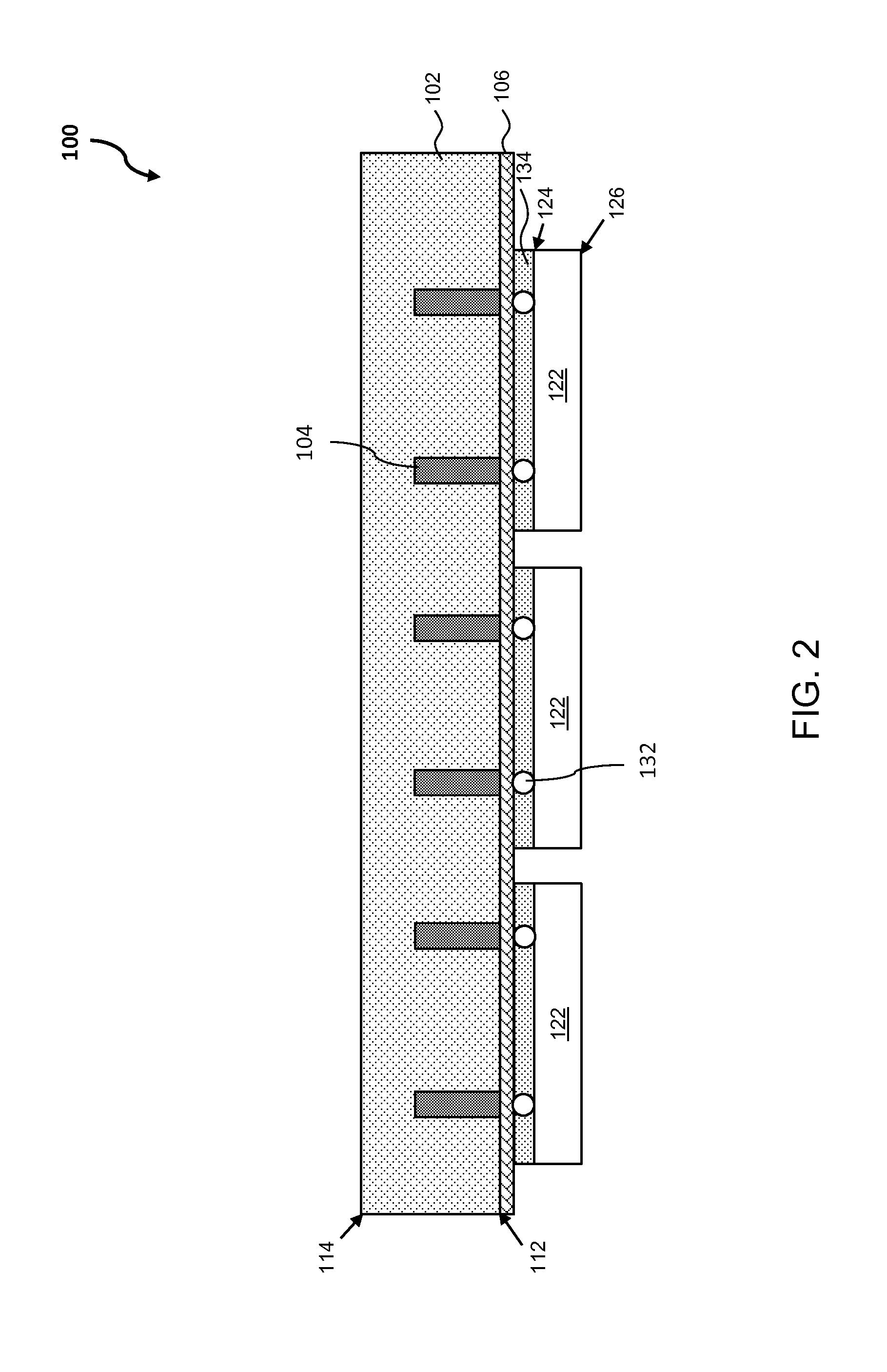
[0017]In addition to the foregoing features, other features and advantages will be understood by persons of ordinary skill in the art having benefit of the present description. The following disclosure provides many different embodiments, or examples, for implementing different features of the provided subject matter. Specific examples of components and arrangements are described below to simplify the present disclosure. These are, of course, merely examples and are not intended to be limiting. For example, the formation of a first feature over or on a second feature in the description that follows may include embodiments in which the first and second features are formed in direct contact, and may also include embodiments in which additional features may be formed between the first and second features, such that the first and second features may not be in direct contact.

[0018]Further, spatially relative terms, such as “beneath,”“below,”“lower,”“above,”“upper” and the like, may be us...


PUM


Abstract

A method of forming a semiconductor package comprises forming one or more first vias in a first side of a substrate and attaching a first side of a first microelectronic element to the first side of the substrate. The first microelectronic element is electrically coupled to at least one of the one or more first vias. The method further comprise obtaining a second microelectronic element including one or more second vias in a first side of the second microelectronic element, and attaching a second side of the substrate to the first side of the second microelectronic element. The second microelectronic element is electrically coupled to at least one of the one or more first vias. Each of one or more connecting elements has a first end attached to a first side of the second microelectronic element and a second end extends beyond a second side of the first microelectronic element.

Description

TECHNICAL FIELD[0001]This present disclosure generally relates to integrated circuits (ICs) packaging technology, and more particularly to IC packaging with high density stacking.BACKGROUND ART[0002]The electronics industry has experienced an ever increasing demand for smaller and faster electronic devices which are simultaneously able to support a greater number of increasingly complex and sophisticated functions. Accordingly, there is a continuing trend in the semiconductor industry to manufacture low-cost, high-performance, and low-power integrated circuits (ICs). Thus far these goals have been achieved in large part by scaling down semiconductor IC dimensions (e.g., minimum feature size) and thereby improving production efficiency and lowering associated costs. However, such scaling has also introduced increased complexity to the semiconductor manufacturing process. Thus, the realization of continued advances in semiconductor ICs and devices calls for similar advances in semicon...

Claims


Application Information

Patent Timeline
IPC IPC(8): H01L25/065H01L21/768H01L21/56H01L23/48H01L23/373H01L23/367H01L23/29H01L23/31H01L25/00H01L23/00
CPCH01L25/0657H01L2224/02372H01L25/0652H01L21/76898H01L21/56H01L24/02H01L23/3731H01L23/367H01L23/29H01L23/3107H01L23/481H01L2225/06541H01L2225/06589H01L2224/0231H01L25/50H01L24/97H01L21/561H01L24/17H01L21/6835H01L24/94H01L25/03H01L25/18H01L2224/13109H01L2224/13111H01L2224/13144H01L2224/14181H01L2224/16145H01L2224/16146H01L2224/17181H01L2224/2929H01L2224/29388H01L2224/32145H01L2224/32225H01L2224/73204H01L2224/92125H01L2224/94H01L2224/97H01L2924/15311H01L2924/18161H01L2225/06513H01L2225/06568H01L2221/68327H01L2221/68331H01L23/3128H01L2224/14155H01L23/295H01L21/563H01L24/13H01L24/14H01L24/81H01L24/92H01L2224/05573H01L2224/05611H01L2224/05647H01L2224/05655H01L2224/05664H01L2224/13124H01L2224/13147H01L2224/13155H01L2224/13164H01L2224/13193H01L2224/16235H01L2224/1703H01L2224/17051H01L2224/2919H01L2224/73104H01L2224/05568H01L2224/0401H01L2224/13022H01L2224/131H01L2224/81H01L2224/83H01L2224/16225H01L2924/00H01L2924/00014H01L2924/0665H01L2924/014
Inventor WOYCHIK, CHARLES G.SITARAM, ARKALGUD R.CAO, ANDREWLEE, BONG-SUB
Owner INVENSAS CORP
Features
  • Generate Ideas
  • Intellectual Property
  • Life Sciences
  • Materials
  • Tech Scout
  • Unparalleled Data Quality
  • Higher Quality Content
  • 60% Fewer Hallucinations
Learn More