
Method for fabricating semiconductor device

Active Publication Date: 2015-12-03
SAMSUNG ELECTRONICS CO LTD
View PDF4 Cites 15 Cited by
  • Summary
  • Abstract
  • Description
  • Claims
  • Application Information

AI Technical Summary

Benefits of technology

This patent describes a method for making a semiconductor device with a three-dimensional channel using uniform ion implantation. The method also allows for the fabrication of transistors with various threshold voltages through one ion implantation process. The method involves forming fins on a substrate, doping the fins simultaneously with impurities, and then removing the doped regions. Additionally, the patent describes a method for making source / drain regions in a removed portion by epitaxial growth. The patent is not limited to a specific set of methodologies and will be useful for those working in the field of semiconductor device fabrication.

Problems solved by technology

However, since a multi-gate transistor has a structure in which a three-dimensional channel is formed in a small area, in certain situations, ion implantation is not easy.
For example, if a general ion implantation process is applied to form the three-dimensional channel, a three-dimensional channel may not be formed because the ion implantation is not performed uniformly.

Method used


Image

  • Method for fabricating semiconductor device
  • Method for fabricating semiconductor device
  • Method for fabricating semiconductor device

Examples


Embodiment Construction

[0020]Advantages and features of the present inventive concept and methods of accomplishing the same may be understood more readily by reference to the following detailed description of various embodiments and the accompanying drawings. The present inventive concept may, however, be embodied in many different forms and should not be construed as being limited to the embodiments set forth herein. Like reference numerals refer to like elements throughout the specification.

[0021]The terminology used herein is for the purpose of describing particular embodiments only and is not intended to be limiting of the inventive concept. As used herein, the singular forms “a”, “an” and “the” are intended to include the plural forms as well, unless the context clearly indicates otherwise. It will be further understood that the terms “comprises” and / or “comprising,” when used in this specification, specify the presence of stated features, integers, steps, operations, elements, and / or components, but...


PUM


Abstract

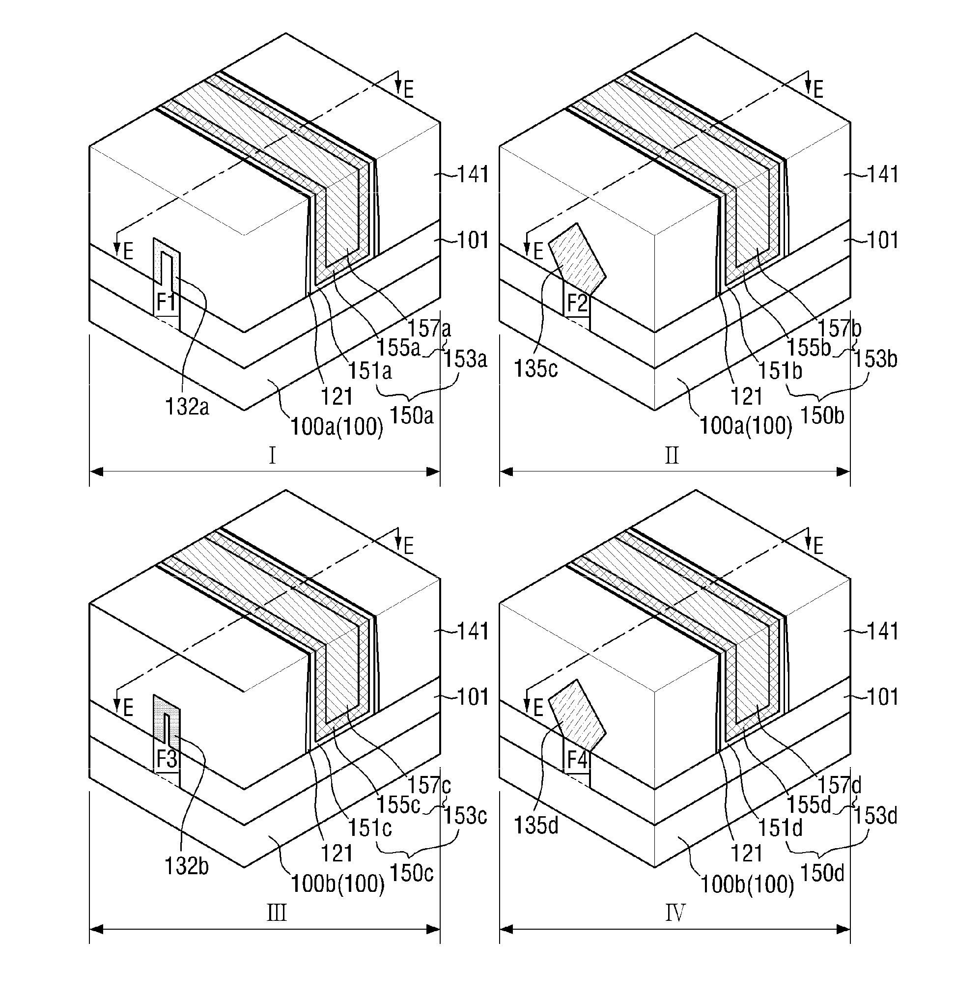
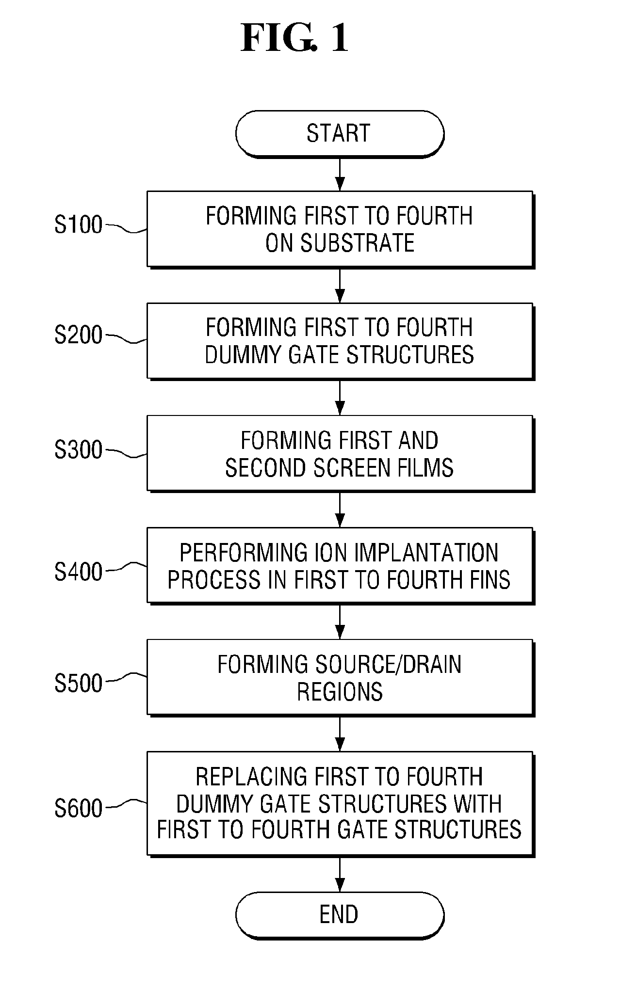
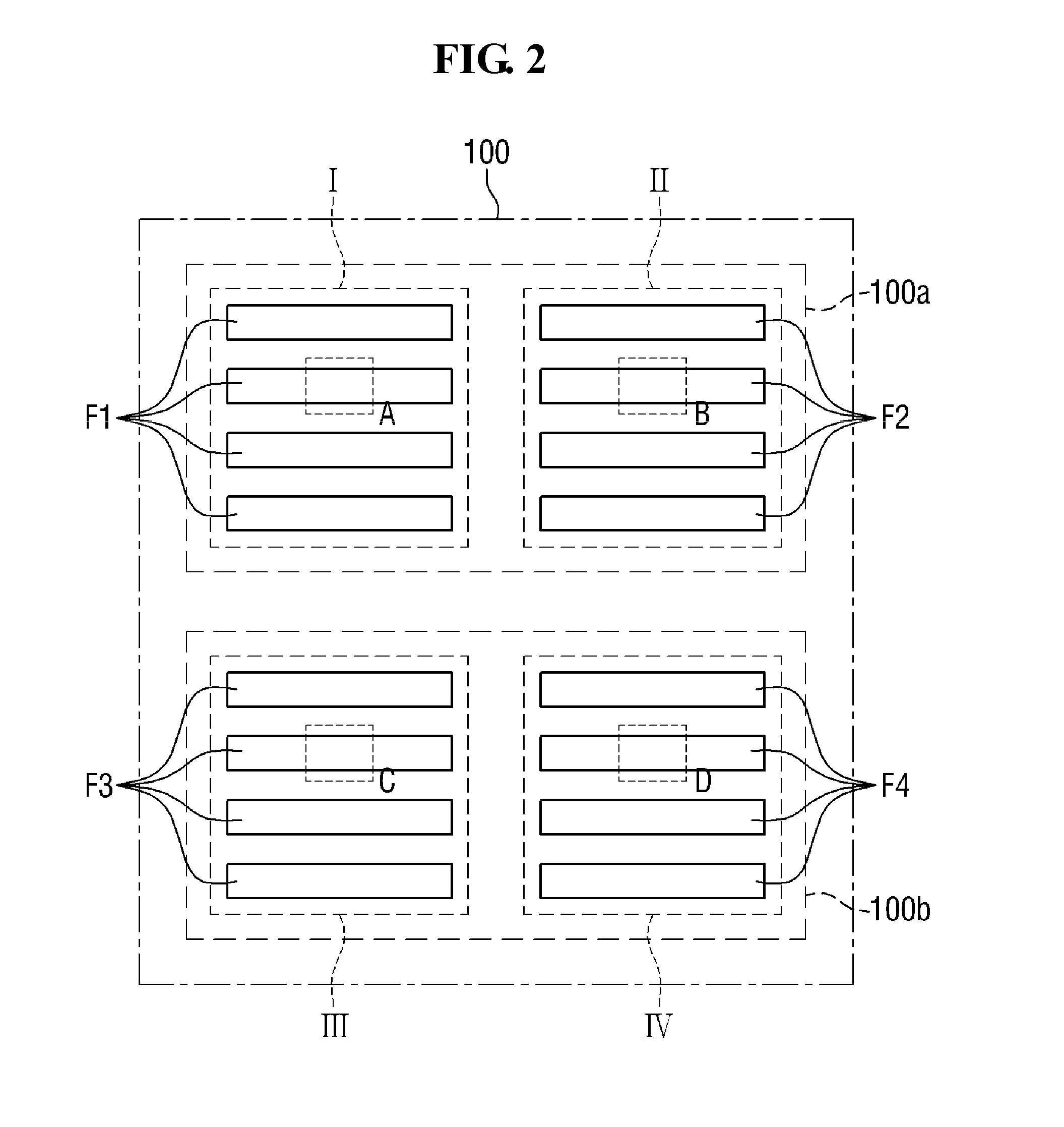
Provided are a method for fabricating a semiconductor device The method for fabricating include providing a substrate including a first region and a second region, the first region including first and second sub-regions, and the second region including third and fourth sub-regions, forming first to fourth fins on the first and second regions to protrude from the substrate, the first fin being formed on the first sub-region, the second fin being formed on the second sub-region, the third fin being formed on the third sub-region, and the fourth fin being formed on the fourth sub-region, forming first to fourth dummy gate structures to intersect the first to fourth fins, the first dummy gate structure being formed on the first fin, the second dummy gate structure being formed on the second fin, the third dummy gate structure being formed on the third fin, and the fourth dummy gate structure being formed on the fourth fin, forming a first doped region in each of the first and second fins and a second doped region in each of the third and fourth fins by doping impurities into the first to fourth fins on both sides of the first to fourth dummy gate structures by performing an ion implantation process simultaneously in the first and second regions; and removing the first doped region of the first fin and the second doped region of the third fin, or removing the first doped region of the second fin and the second doped region of the fourth fin.

Description

CROSS-REFERENCE TO RELATED APPLICATION[0001]This application claims priority from Korean Patent Application No. 10-2014-0063746 filed on May 27, 2014 in the Korean Intellectual Property Office, and all the benefits accruing therefrom under 35 U.S.C. 119, the contents of which in its entirety are herein incorporated by reference.BACKGROUND[0002]1. Field of the Invention[0003]The present inventive concept relates to a method for fabricating a semiconductor device.[0004]2. Description of the Related Art[0005]As one of scaling techniques for increasing the density of an integrated circuit device, there has been proposed a multi-gate transistor in which a silicon body having a fin shape or nanowire shape is formed on a substrate and a gate is formed on the surface of the silicon body.[0006]In such a multi-gate transistor, since a three-dimensional channel is used, scaling is relatively easy. Further, although the gate length of the multi-gate transistor is not increased, the current cont...

Claims


Application Information

Patent Timeline
IPC IPC(8): H01L29/66H01L21/265H01L21/8238
CPCH01L29/66803H01L21/823821H01L29/6681H01L21/26586H01L21/823814H01L21/823418H01L21/823431H01L27/0924H01L29/165H01L29/66545H01L29/7848H01L29/785
Inventor SONG, SEUNG-HYUNSON, NAK-JINLEE, KWANG-SEOKJEONG, CHANG-WOOKKWON, UI-HUIKIM, DONG-WONPARK, YOUNG-KWANLEE, KEUN-HO
Owner SAMSUNG ELECTRONICS CO LTD
Learn More