Display

a technology of display and display plate, applied in the field of display plate, can solve the problems of difficult to reduce disturbances in image display, degrade the transmittance of display plate, and deterioration of display optical properties, so as to facilitate static electricity discharge and reduce the resistance of the sheet of conductive pattern

Active Publication Date: 2015-12-24
JAPAN DISPLAY INC
View PDF1 Cites 16 Cited by
  • Summary
  • Abstract
  • Description
  • Claims
  • Application Information

AI Technical Summary

Benefits of technology

[0008]In the technique recited in the above Patent Literature 2, static electricity applied to the display with touch detection functions is moved from the conductive layer to the touch detecting electrodes, and static electricity moved to the touch detecting electrodes is moved to a grounding line or the like of the display with touch detection functions. In this manner, by providing a conductive layer or a conductive pattern such as touch detecting electrodes or the like on the opposing substrate, static electricity applied to the display can be discharged to the exterior of the display through the conductive layer or the conductive pattern such as touch detecting electrodes or the like provided on the opposing substrate. Further, for easily discharging static electricity to the exterior of the display, it is necessary to reduce a sheet resistance of the conductive pattern.

Problems solved by technology

However, when either the thickness of the conductive pattern is increased or the area ratio of the conductive pattern is increased, the transmittance of the display is degraded, and optical properties of the display are deteriorated.
Accordingly, it is difficult to reduce disturbances in display of images caused through static electricity without deteriorating optical properties.

Method used


Image

  • Display
  • Display
  • Display

Examples


first embodiment

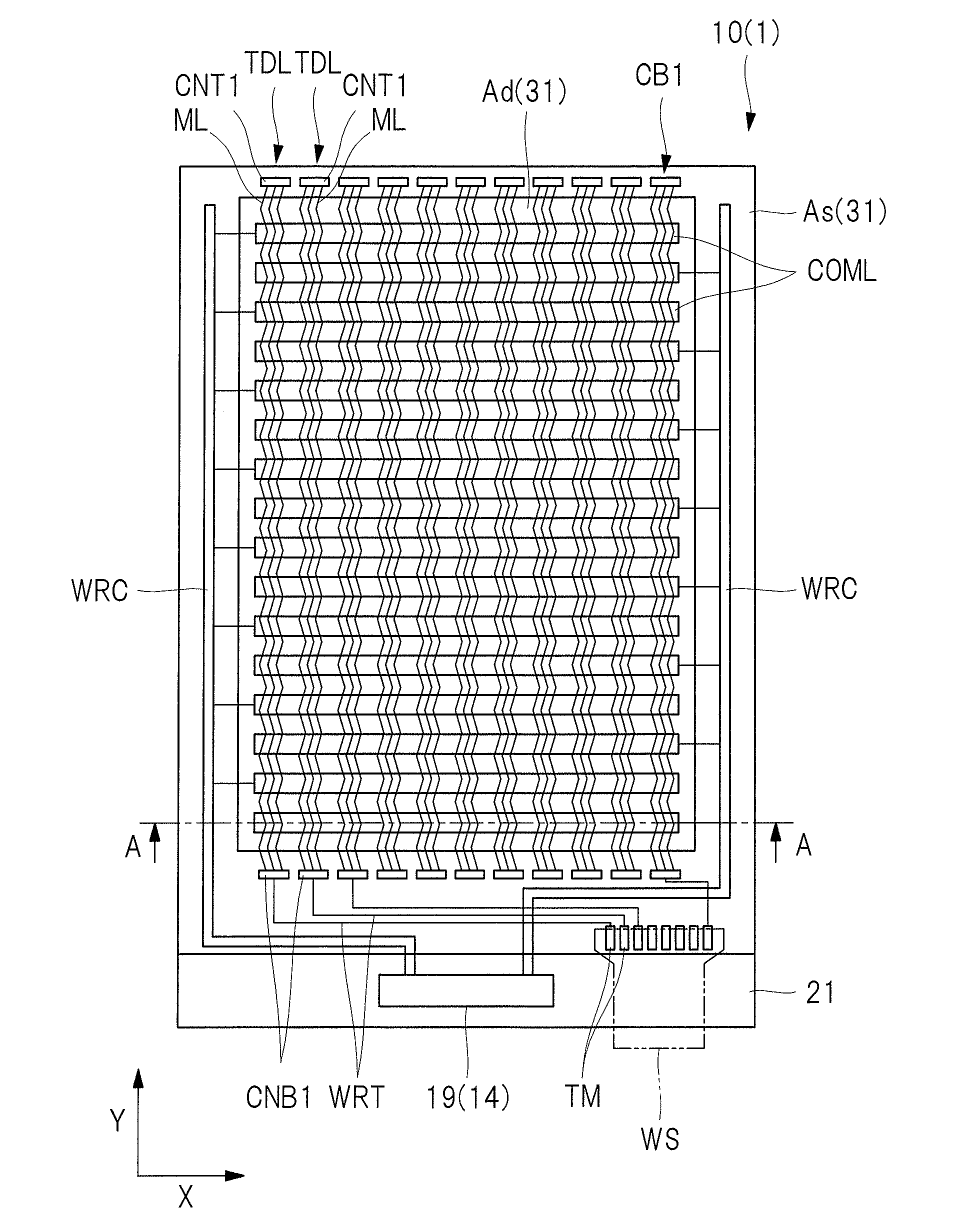
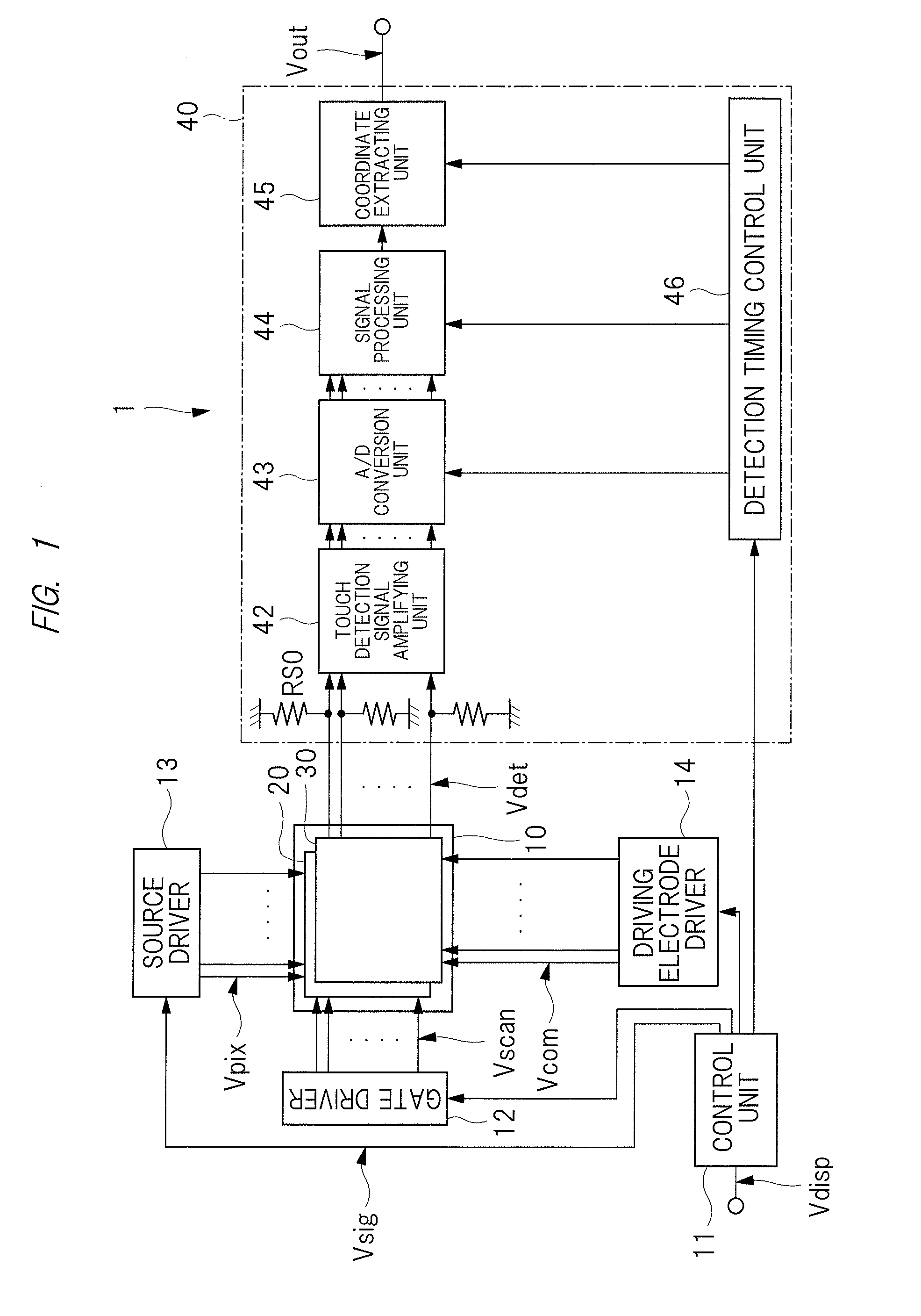
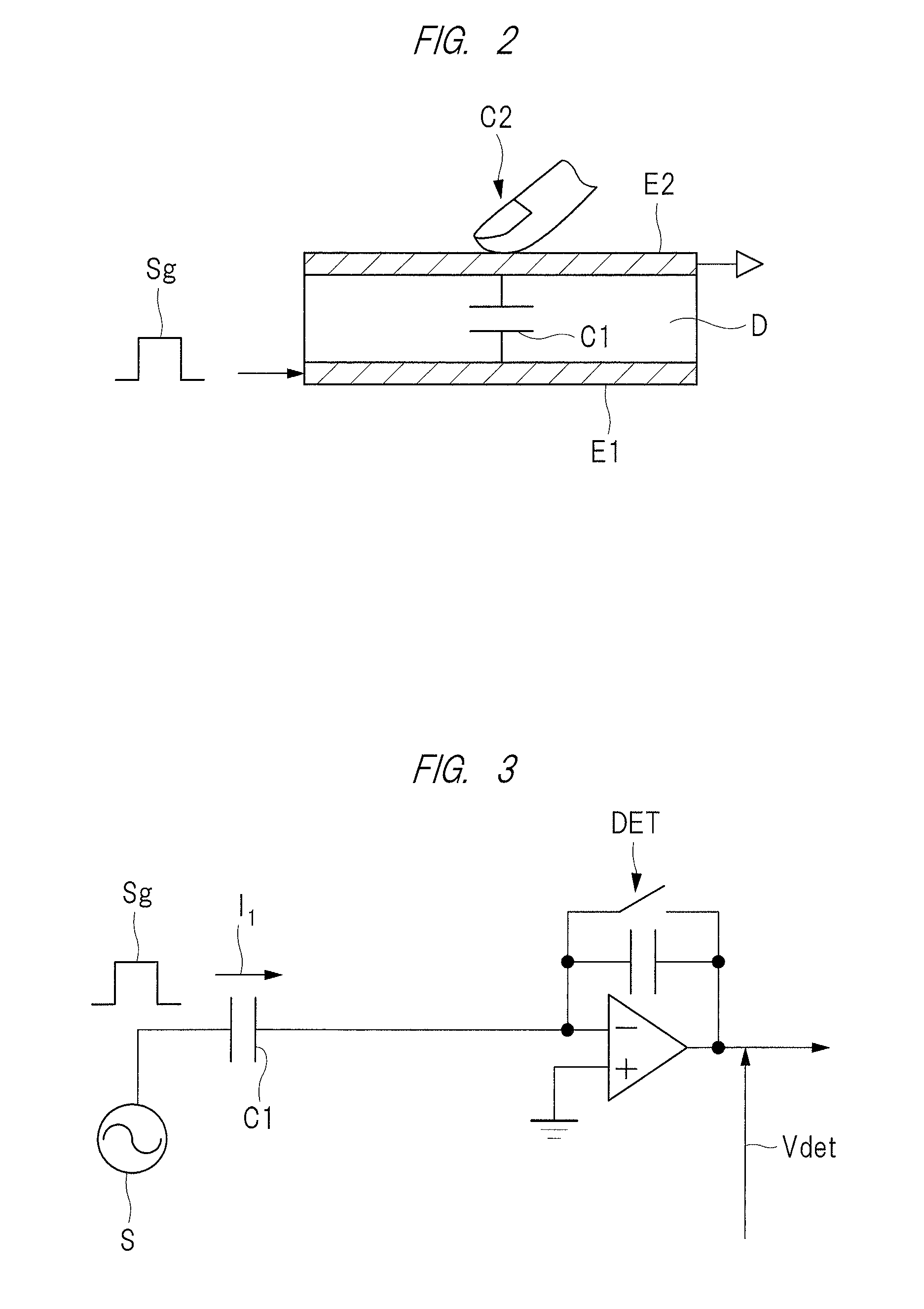
[0042]First, an example in which a display provided with a touch panel as an input device is applied to a liquid crystal display with touch detection functions of in cell type will be explained as the first embodiment. In the present descriptions, an input device is an input device detecting electrostatic capacities which change at least depending on capacities of objects that approach or contact electrodes. Further, a liquid crystal display with touch detection functions is a liquid crystal display provided with detecting electrodes for touch detection on either an array substrate 2 or an opposing substrate 3 which form the display. Moreover, in the first embodiment, a display with touch detection functions of in cell type characterized in that driving electrodes operate as driving electrodes of the display and operate as driving electrodes of the input device will be described.

[0043]

[0044]First, the overall configuration of the display of the first embodiment will be explained wit...

second embodiment

[0201]In the first embodiment, static electricity applied from the exterior of the display device with touch detection functions is discharged to the exterior of the display through the conductive pattern provided in the display region. In contrast thereto, in the second embodiment, static electricity applied from the exterior of the display with touch detection functions is discharged to the exterior of the display through the conductive pattern provided in the display region and through the conductive pattern provided in the peripheral region.

[0202]The overall configuration of the display of the second embodiment might be the same as the overall configuration of the display of the first embodiment and explanations thereof will be omitted.

[0203]

[0204]FIG. 17 is a plan view showing one example of a module mounted with the display according to the second embodiment. FIG. 18 is a sectional view showing a display device with touch detection functions of the display according to the sec...

third embodiment

[0225]In the first embodiment, the polarizing plate provided on the opposite side of the array substrate with the opposing substrate being interposed therebetween includes a conductive layer. In contrast thereto, in the third embodiment, the polarizing plate provided on the opposite side of the array substrate with the opposing substrate being interposed therebetween does not include a conductive layer, but a protection layer provided to cover the conductive pattern functions as a conductive layer.

[0226]The overall configuration of the display of the third embodiment might be the same as the overall configuration of the display of the first embodiment and explanations thereof will be omitted.

[0227]

[0228]FIG. 20 is a sectional view showing a display device with touch detection functions of the display according to the third embodiment. FIG. 21 is a sectional view schematically showing movements of static electricity in the display device with touch detection functions of the display ...


PUM

PropertyMeasurementUnit
sheet resistanceaaaaaaaaaa

Abstract

To reduce disturbances in display of images due to static electricity without deteriorating optical properties in a display. The display includes a conductive pattern provided on the upper surface of the substrate, a protection layer provided on the upper surface of the substrate to cover the conductive pattern, and a conductive layer provided on the protection layer. The sheet resistance of the conductive pattern is not more than 8Ω/square. A ratio of the total sum of areas of portions of the plurality of sub-pixels that overlap the conductive pattern in a plan view to the total sum of the areas of the plurality of sub-pixels is 1 to 22%. A sheet resistance of the conductive layer is higher than the sheet resistance of the conductive pattern.

Description

CROSS-REFERENCE TO RELATED APPLICATION[0001]The present application claims priority from Japanese Patent Application No. 2014-125011 filed on Jun. 18, 2014, the content of which is hereby incorporated by reference into this application.TECHNICAL FIELD OF THE INVENTION[0002]The present invention relates to a display, and particularly to a display including a liquid crystal layer.BACKGROUND OF THE INVENTION[0003]Displays such as liquid crystal displays include, for instance, an array substrate, an opposing substrate disposed to oppose the array substrate, and a liquid crystal layer interposed between the array substrate and the opposing substrate. The array substrate or the opposing substrate is provided with a light shielding portion having a lattice-like shape in a plan view, and a plurality of pixels are divided by the light shielding portion. The array substrate is formed, for instance, with a thin film transistor (TFT) as a switching element.[0004]In such a display, in each of th...

Claims


Application Information

Patent Timeline
Patent Type & Authority Applications(United States)
IPC IPC(8): G06F3/044G02F1/1335G02F1/1343G02F1/1333
CPCG06F3/044G02F1/13338G02F2202/28G02F1/134309G02F2001/133545G02F1/133528G02F1/136204G06F3/0412G06F3/0445G02F1/134372
Inventor IKEDA, MASANOBUISHIZAKI, KOJIKURASAWA, HAYATOWATANABE, YOSHIHIROISHIGAKI, TOSHIMASASONODA, DAISUKEIDE, TATSUYA
Owner JAPAN DISPLAY INC
Why Eureka
Try Eureka