Array substrate and display device

a display device and substrate technology, applied in the field of display technology, can solve the problem that the display performance of the display panel cannot be further improved, and achieve the effect of improving the display performance of the display device and the aperture ratio of the display devi

Active Publication Date: 2015-12-24
BOE TECH GRP CO LTD
View PDF3 Cites 10 Cited by
  • Summary
  • Abstract
  • Description
  • Claims
  • Application Information

AI Technical Summary

Benefits of technology

[0022]Advantages of the invention are as follows: in the array substrate of the invention, both the control section and the display section in each pixel unit are provided to be symmetrically distributed with the central line of the gate line as a sharing symmetry axis, the control section is provided at a cross-point of the gate line and the data line, and the display section is provided at a region of the pixel unit other than the region where the control section is located, the gate lines are at least partially overlapped with the data lines, and the shared source is at least partially overlapped with the corresponding gate line, so that the space occupied by the control section is largely reduced and the area occupied by the display section may be increased accordingly, and thus the aperture ratio of the array substrate is increased and the display performance of the array substrate is improved.
[0023]In the display device of the invention, by adopting the above array substrate, the aperture ratio of the display device is largely increased and the display performance of the display device is improved.

Problems solved by technology

Since an effective region for transmitting light and displaying is mainly formed by the region corresponding to the pixel electrode 52, therefore the aperture ratio (the ratio of the effective light-transmissive region to the area of the pixel unit) of the array substrate is relatively small, and thus the aperture ratio of the entire display panel is small, which results in the fact that the display performance of the display panel cannot be further improved.

Method used


Image

  • Array substrate and display device
  • Array substrate and display device
  • Array substrate and display device

Examples


embodiment 1

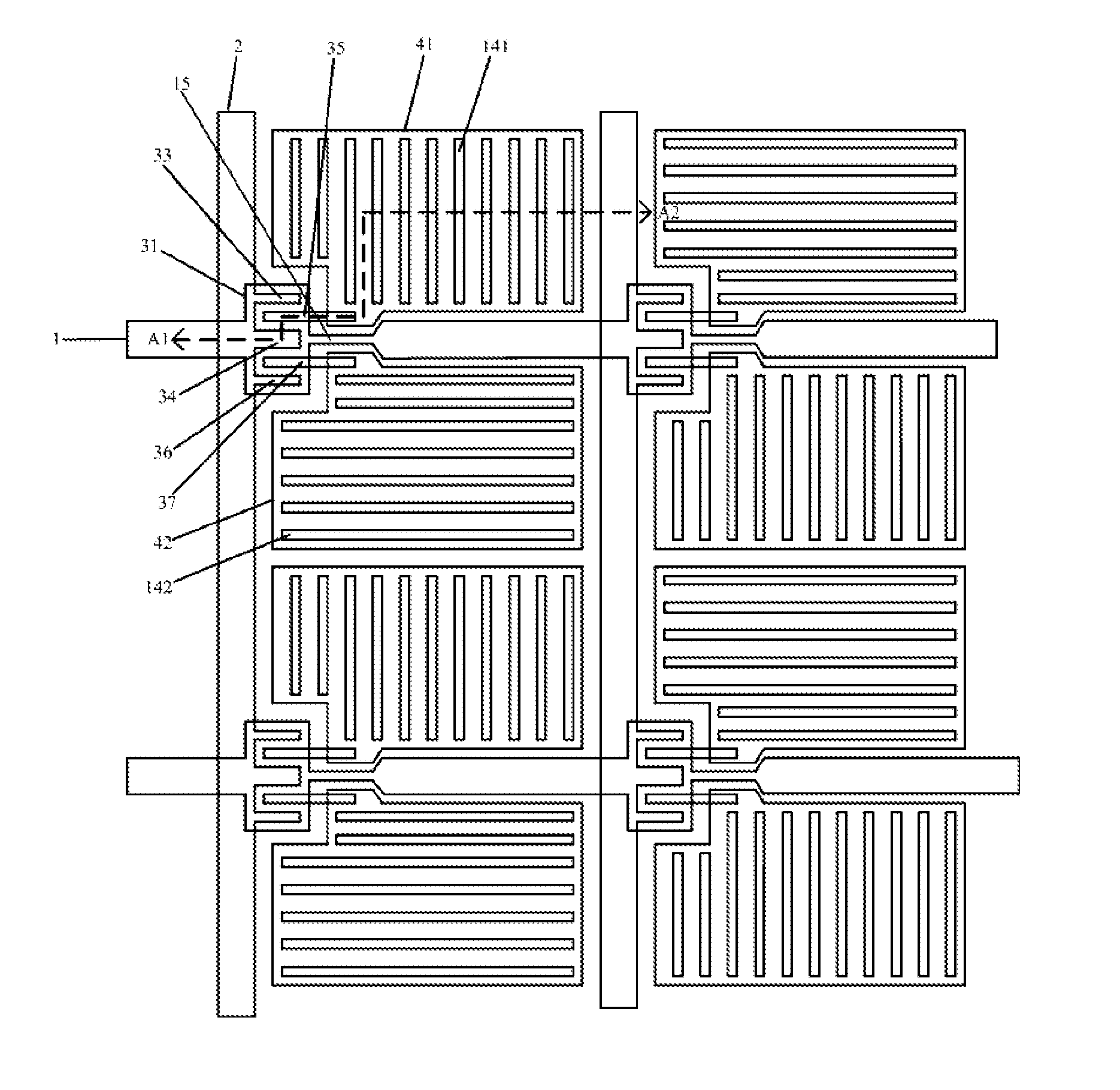
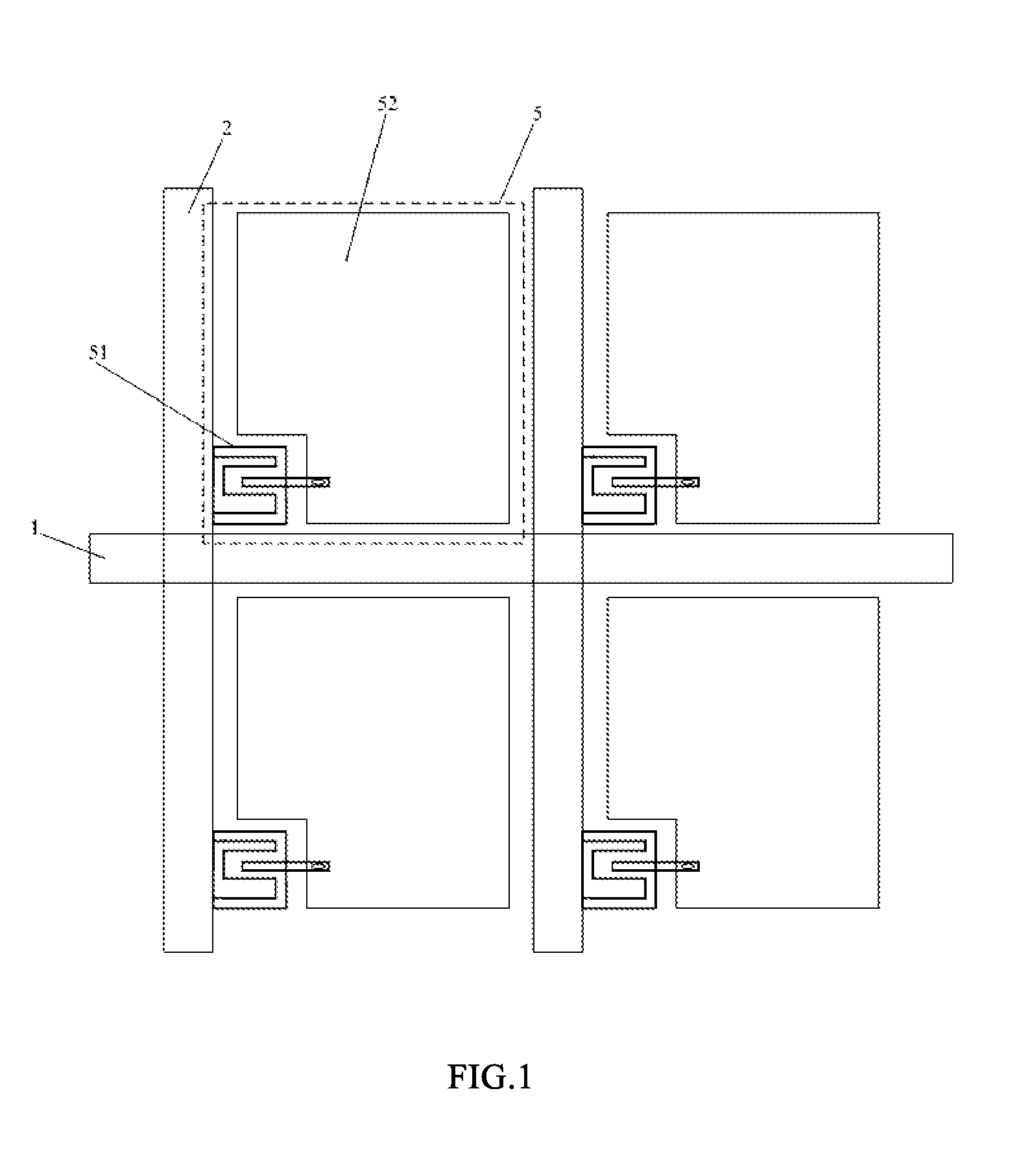
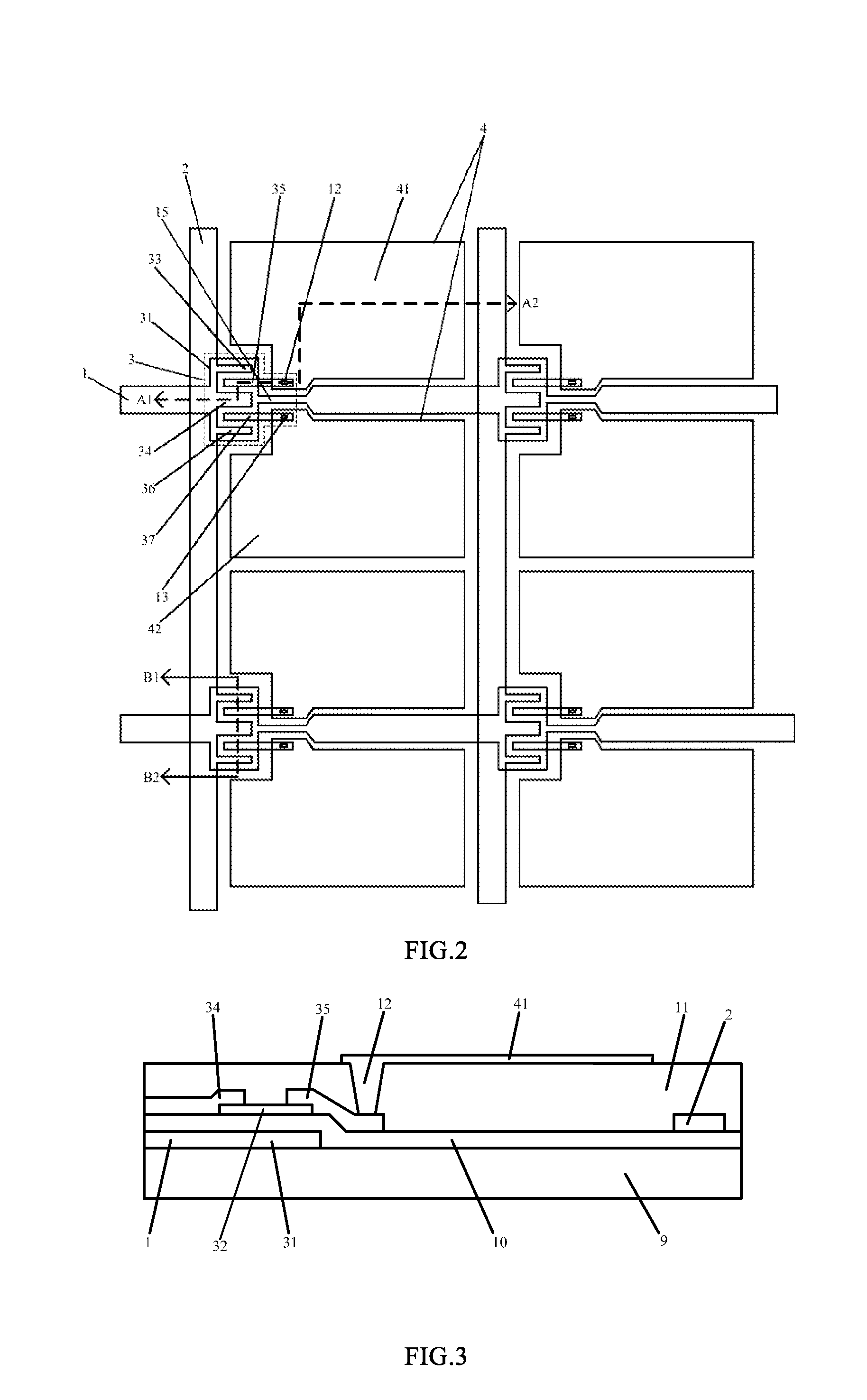
[0032]The embodiment provides an array substrate, which comprises, as shown in FIG. 2, a plurality of gate lines 1 and a plurality of data lines 2 which are arranged crosswise and are insulated from each other. The array substrate also comprises a plurality of pixel units which are provided at regions defined by the gate lines 1 and the data lines 2. The pixel unit comprises a control section 3 and a display section 4 each of which is symmetrically distributed with the central line of the corresponding gate line 1 as a symmetry axis, the control section 3 is provided at a cross-point of the gate line 1 and a corresponding data line 2, and the display section 4 is provided at a region of the pixel unit other than the region where the control section is located. The control section 3 is connected to the display section 4 so as to control the display section 4 for display.

[0033]As shown in FIG. 2, FIG. 3 and FIG. 4, the control section 3 comprises a first thin film transistor and a sec...

embodiment 2

[0056]Unlike the embodiment 1, in an array substrate in the present embodiment, both of the first pixel electrode and the second pixel electrode are partially overlapped with the gate line; alternatively, the first pixel electrode and the second pixel electrode are connected as a whole, and completely cover part of the gate line corresponding to the first pixel electrode and the second pixel electrode.

[0057]With such configuration, areas of the first pixel electrode and the second pixel electrode may be further increased, and thus the aperture ratio of the array substrate may be further increased.

[0058]Other structures, manufacturing method and materials of the array substrate in the present embodiment are the same as those in the embodiment 1, and will not be described herein.

embodiment 3

[0059]The present embodiment provides an array substrate, unlike the embodiments 1 and 2, as shown in FIG. 5 and FIG. 6, the first pixel electrode 41 and the second pixel electrode 42 are provided in the same layer and above the gate insulating layer 10, and a common electrode layer 14 is provided above the passivation layer 11, wherein the common electrode layer 14 is provided with first slits 141 and second slits 142 therein, the first slits 141 are correspondingly provided above the first pixel electrode 41, and the second slits 142 are correspondingly provided above the second pixel electrode 42.

[0060]As the first pixel electrode 41 and the second pixel electrode 42 above the gate insulating layer 10 may directly contact the first drain 35 and the second drain 37 and connected thereto, respectively, in the present embodiment, it is unnecessary to provide the first via and the second via in the passivation layer 11 and the resin layer.

[0061]With above configuration, the first pix...


PUM


Abstract

The invention provides an array substrate and a display device. The array substrate comprises a plurality of gate lines and a plurality of data lines which are arranged crosswise and are insulated from each other, and a plurality of pixel units, wherein each pixel unit comprises a control section and a display section, each of which is symmetrically distributed with the central line of a corresponding gate line as a symmetry axis, the control section is located at a cross-point of the gate line and the data line, and is at least partially overlapped with the gate line and the data line, the display section is located at a region defined by the gate line and the data line; and the control section is connected to the display section to control the display section for display. In the present invention, the aperture ratio of the array substrate is increased.

Description

TECHNICAL FIELD[0001]The invention relates to the field of display technology, and in particular to an array substrate and a display device.BACKGROUND ART[0002]Liquid Crystal Displays (LCDs) have become mainstream products in the present flat panel display devices due to their small volume, low power consumption, no radiation and so on. Liquid crystal display technology is widely applied to television, mobile phone and public information display.[0003]A liquid crystal display panel is a main component of a liquid crystal display device, and the liquid crystal display panel comprises an array substrate and a color filter substrate. The array substrate comprises a plurality of gate lines and a plurality of data lines which are arranged crosswise and overlap with each other at cross-points, and pixel units are provided in regions enclosed by adjacent gate lines and data lines. The pixel unit comprises a thin film transistor and a pixel electrode, and the thin film transistor is used to...

Claims


Application Information

Patent Timeline
Patent Type & Authority Applications(United States)
IPC IPC(8): H01L27/12
CPCH01L27/124
Inventor CHENG, HONGFEILI, WENBOQIAO, YONGXIAN, JIANBOLI, PAN
Owner BOE TECH GRP CO LTD
Why Eureka
Try Eureka