Semiconductor structure and method for manufacturing the same

a technology of semiconductors and semiconductors, applied in the direction of semiconductor devices, electrical equipment, transistors, etc., can solve the problems of increasing manufacturing costs and wasting more wafer area than necessary, and achieve the effects of avoiding wasting wafer area, improving overall performance of cmos circuits, and less difficulty in lithography

Inactive Publication Date: 2015-12-31
INST OF MICROELECTRONICS CHINESE ACAD OF SCI
View PDF1 Cites 9 Cited by
  • Summary
  • Abstract
  • Description
  • Claims
  • Application Information

AI Technical Summary

Benefits of technology

[0018]As compared to the prior art, the technical solution provided by the present invention has the following advantages.
[0019]It is possible to form two parallel semiconductor fins with different crystal planes on the same substrate by changing crystal orientation of a part of the substrate. The two semiconductor fins have {100} cryst...

Problems solved by technology

Because fin structures of PMOS and NMOS devices are not parallel, difficulty in lithography may ...

Method used


Image

  • Semiconductor structure and method for manufacturing the same
  • Semiconductor structure and method for manufacturing the same
  • Semiconductor structure and method for manufacturing the same

Examples


Embodiment Construction

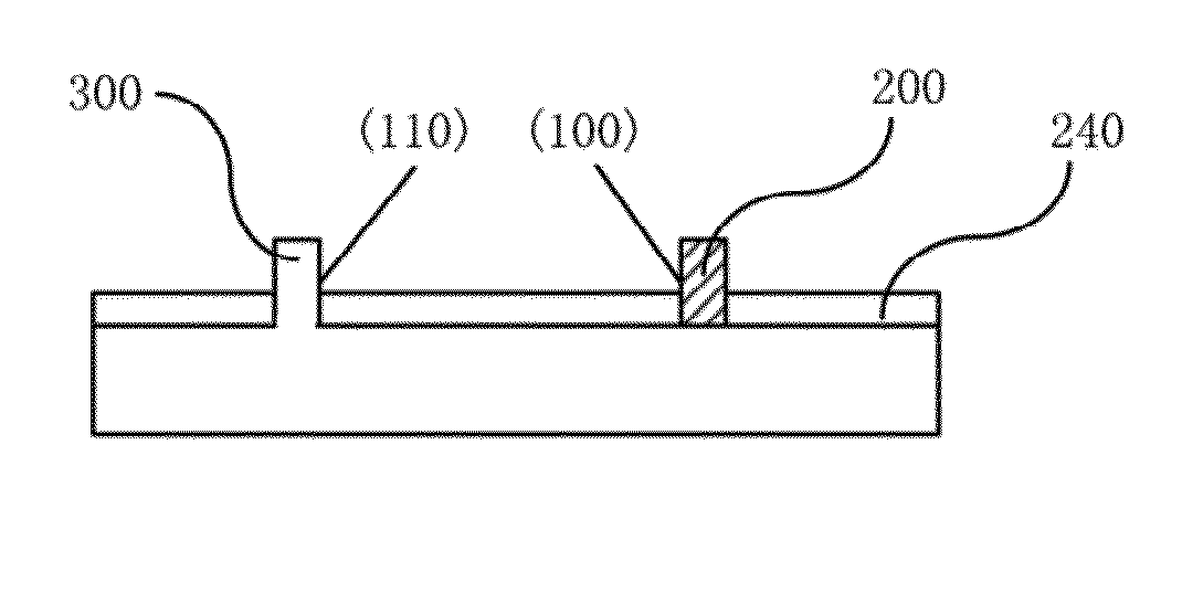
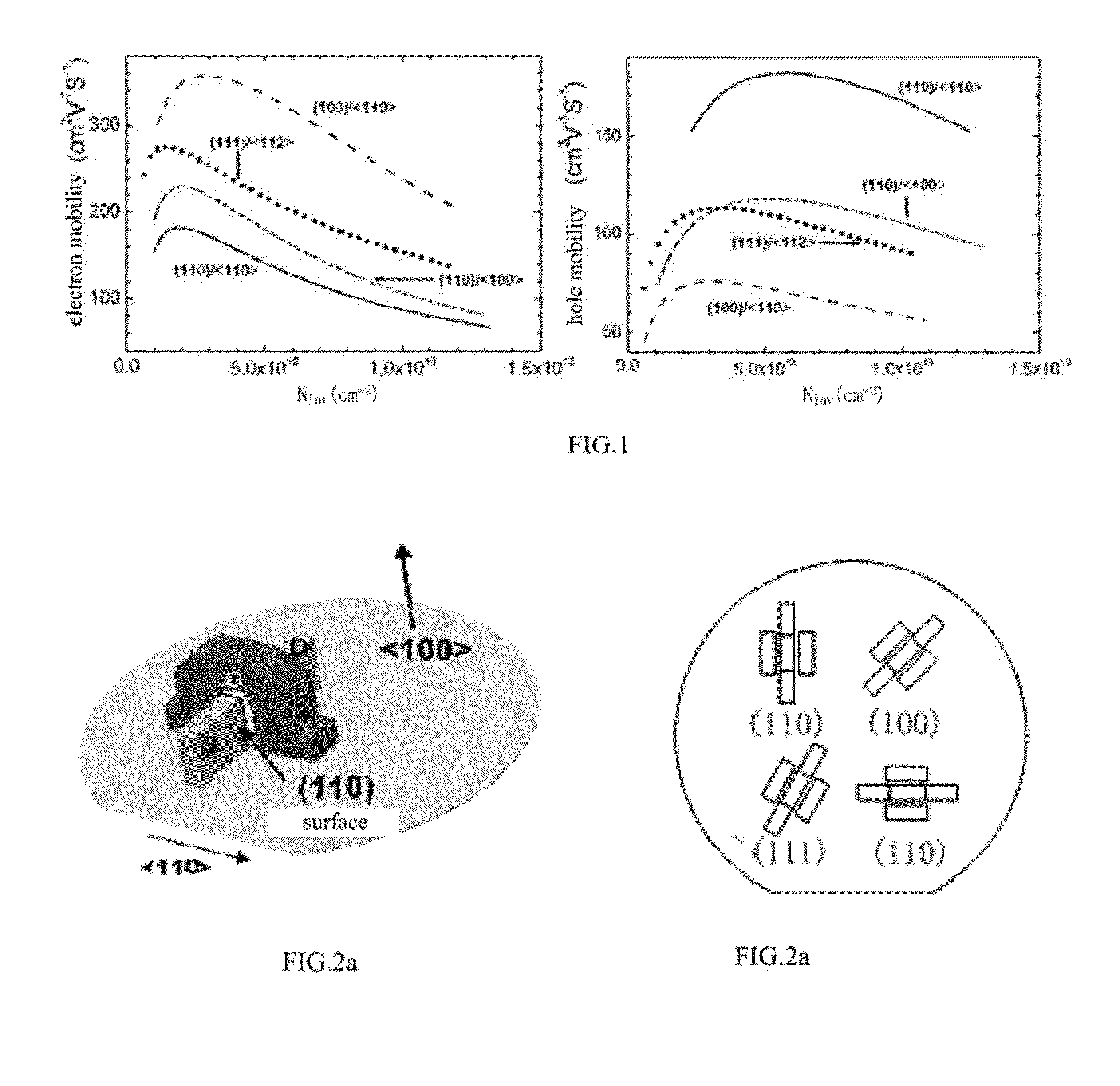
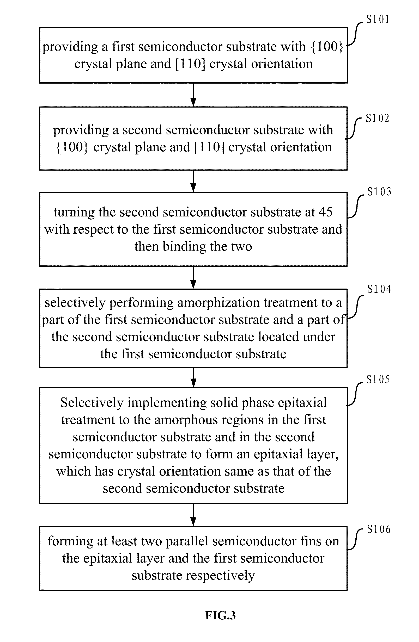
[0025]Here below, the present invention is described in detail in view of embodiments illustrated in the accompanying drawings. However, it should be understood that the description is exemplary, and are not intended to limit the scope of the present invention.

[0026]Various embodiments or examples are provided here below to implement different structures of the present invention. To simplify disclosure of the present invention, description of components and arrangements of specific examples is given below. Of course, they are illustrative only, and are not intended to limit the present invention. Moreover, in the present invention, reference numbers and / or letters may be repeated in different embodiments. Such repetition is for purposes of simplification and clarity, and does not denote any relationship between respective embodiments and / or arrangements under discussion. Furthermore, the present invention provides various examples for various processes and materials. However, it is ...


PUM


Abstract

The present invention provides a semiconductor structure, which comprises a semiconductor substrate and at least two semiconductor fins located on the semiconductor substrate, wherein: the at least two semiconductor fins are parallel to each other; and the parallel sidewall surfaces of the at least two semiconductor fins have different crystal planes. The present invention further provides a method for manufacturing aforesaid semiconductor structure. The technical solution provided in the present invention exhibits following advantages: it makes possible to form two parallel semiconductor fins with different sidewall crystal planes on the same substrate through changing crystal orientation of a part of the substrate; the two semiconductor fins individually have {100} sidewall crystal plane and {110} sidewall crystal plane, and are applied for forming NMOS and PMOS devices respectively; in this way, the overall performance of CMOS circuits is improved; besides, the two semiconductor fin structures are parallel to each other, such that it becomes less difficult to perform lithography and avoids wasting of wafer area.

Description

[0001]The present application claims priority benefit of Chinese patent application No. 201210276441.5, filed on 3 Aug. 2012, entitled “SEMICONDUCTOR STRUCTURE AND METHOD FOR MANUFACTURING THE SAME”, which is herein incorporated by reference in its entirety.FIELD OF THE INVENTION[0002]The present invention relates to a semiconductor structure with Fins and a method for manufacturing the same, and specifically, to a semiconductor fins applied in FinFETs and a method for manufacturing the same.BACKGROUND OF THE INVENTION[0003]The traditional process for manufacturing bulk Si FinFETs (Fin Filed Effect Transistors) comprises forming an extended thin fin on a substrate, then forming a gate dielectric layer and a gate, and thereby forming a transistor. However, as revealed from researches, PMOS has highest hole mobility when transistor channels are directed along [110] crystal orientation of {110 } crystal plane, while NMOS has highest electron mobility when transistor channels are direct...

Claims


Application Information

Patent Timeline
IPC IPC(8): H01L27/092H01L21/8238H01L21/02H01L21/265H01L21/302H01L29/04H01L21/324
CPCH01L21/823807H01L21/823821H01L21/02002H01L29/045H01L21/02433H01L21/265H01L21/302H01L21/324H01L21/823828H01L27/0924H01L21/185
Inventor YIN, HAIZHOULIU, YUNFEI
Owner INST OF MICROELECTRONICS CHINESE ACAD OF SCI
Why Eureka
Try Eureka