Signal Response Metrology Based On Measurements Of Proxy Structures

a proxy structure and signal response technology, applied in the field of metalrology systems and methods, can solve the problems of lack of sensitivity of optical cd and film metrologies to many structures employed in multiple patterning techniques, lack of high throughput (e.g., optical) measurement solutions, and inability to meet the design rules of specialized target structures, etc., to achieve the effect of reducing computation and user time, and improving prediction results

Active Publication Date: 2016-01-07
KLA TENCOR TECH CORP
View PDF8 Cites 55 Cited by
  • Summary
  • Abstract
  • Description
  • Claims
  • Application Information

AI Technical Summary

Benefits of technology

[0022]The trained measurement models described herein receive optical measurement data directly as input and provide values of parameters of inte

Problems solved by technology

However, optical CD and film metrologies suffer from lack of sensitivity to many structures employed in multiple patterning techniques, buried structures, in particular.
For some structural parameters, such as edge placement error (EPE), there is currently no high throughput (e.g., optical) measurement solution.
Unfortunately, these specialized target structures often do not conform to the design rules of the particular semiconductor manufacturing process being employed to generate the electronic device.
This leads to errors

Method used


Image

  • Signal Response Metrology Based On Measurements Of Proxy Structures
  • Signal Response Metrology Based On Measurements Of Proxy Structures
  • Signal Response Metrology Based On Measurements Of Proxy Structures

Examples


Embodiment Construction

[0035]Reference will now be made in detail to background examples and some embodiments of the invention, examples of which are illustrated in the accompanying drawings.

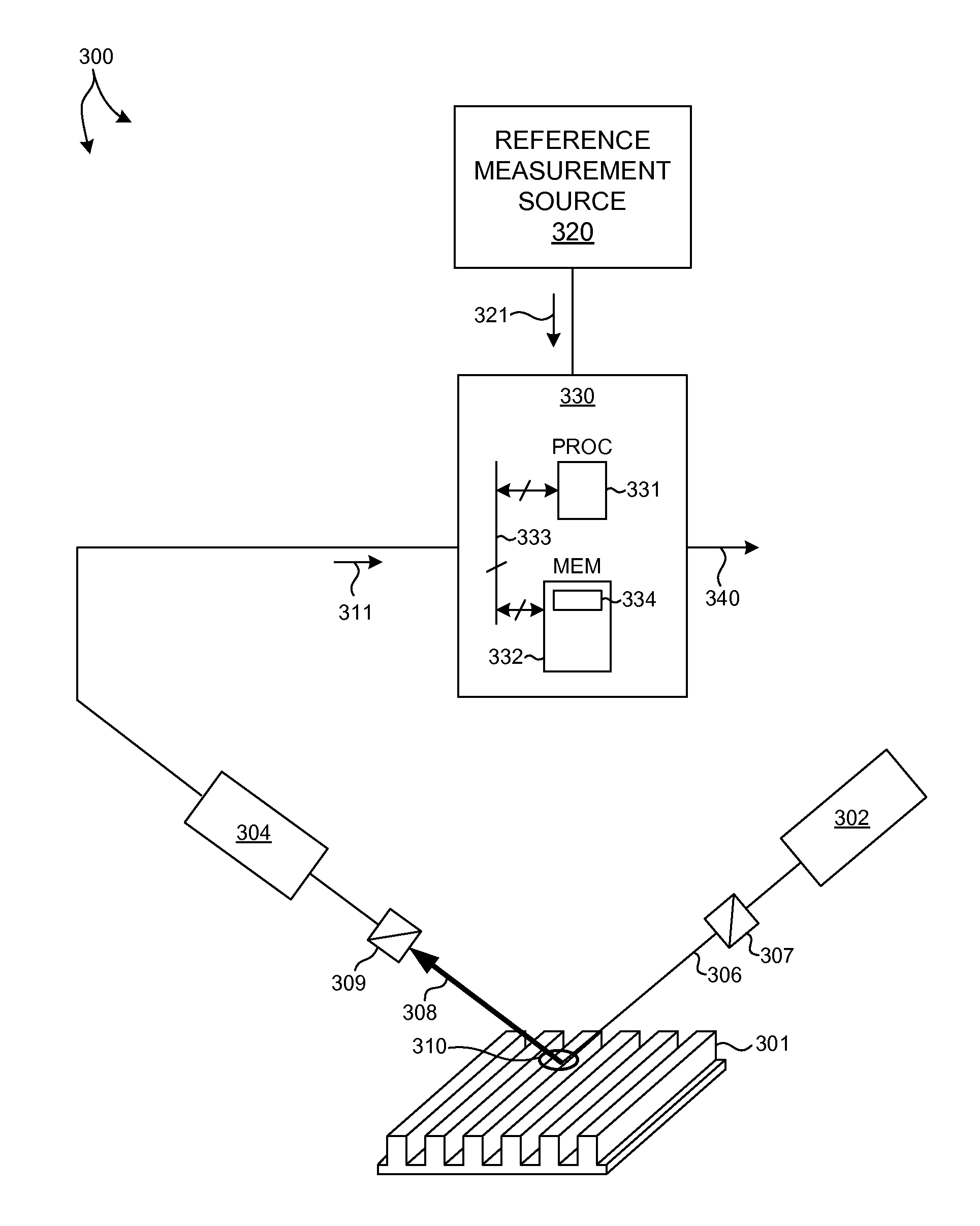
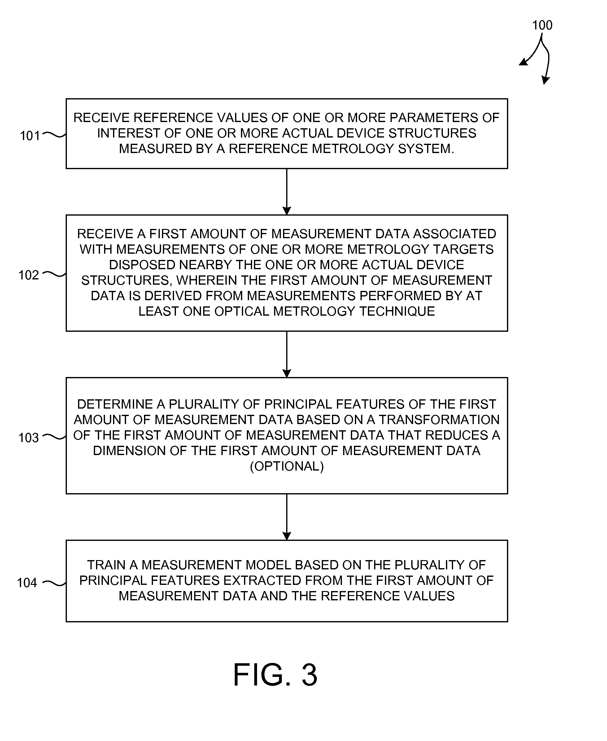
[0036]Methods and systems for estimating values of parameters of interest of actual device structures based on optical measurements of nearby metrology targets are presented herein. High throughput, inline metrology techniques (e.g., optical scatterometry, imaging overlay, or other techniques) are employed to measure metrology targets located near actual device structures. The high throughput, inline metrology techniques typically lack measurement sensitivity to the parameters of interest for the actual device structures, but have sufficient sensitivity to parameters of nearby metrology targets. The optical metrology targets are located sufficiently close to the actual device structures of interest to ensure that spatial process variations do not significantly affect the robustness of the measurement algorithm. Measur...


PUM


Abstract

Methods and systems for estimating values of parameters of interest of actual device structures based on optical measurements of nearby metrology targets are presented herein. High throughput, inline metrology techniques are employed to measure metrology targets located near actual device structures. Measurement data collected from the metrology targets is provided to a trained signal response metrology (SRM) model. The trained SRM model estimates the value of one or more parameters of interest of the actual device structure based on the measurements of the metrology target. The SRM model is trained to establish a functional relationship between actual device parameters measured by a reference metrology system and corresponding optical measurements of at least one nearby metrology target. In a further aspect, the trained SRM is employed to determine corrections of process parameters to bring measured device parameter values within specification.

Description

CROSS REFERENCE TO RELATED APPLICATION[0001]The present application for patent claims priority under 35 U.S.C. §119 from U.S. provisional patent application Ser. No. 62 / 021,659, entitled “Metrology and Method to Control Process Parameters to Improve Semiconductor Device Yield and Edge Placement Errors,” filed Jul. 7, 2014, the subject matter of which is incorporated herein by reference in its entirety.TECHNICAL FIELD[0002]The described embodiments relate to metrology systems and methods, and more particularly to methods and systems for improved measurement of semiconductor structures.BACKGROUND INFORMATION[0003]Semiconductor devices such as logic and memory devices are typically fabricated by a sequence of processing steps applied to a specimen. The various features and multiple structural levels of the semiconductor devices are formed by these processing steps. For example, lithography among others is one semiconductor fabrication process that involves generating a pattern on a sem...

Claims


Application Information

Patent Timeline
IPC IPC(8): G01B11/14G01B11/06
CPCG01B11/0616G01B11/14H01L22/12G03F7/705G03F7/7065H01L22/24
Inventor SHCHEGROV, ANDREI V.DZIURA, THADDEUS GERARDPANDEV, STILIAN IVANOVPOSLAVSKY, LEONID
Owner KLA TENCOR TECH CORP
Why Eureka
Try Eureka