Liquid crystal display device conductive tape attaching structure, liquid crystal display device, and manufacturing method thereof
- Summary
- Abstract
- Description
- Claims
- Application Information
AI Technical Summary
Benefits of technology
Problems solved by technology
Method used
Image

Examples
first exemplary embodiment
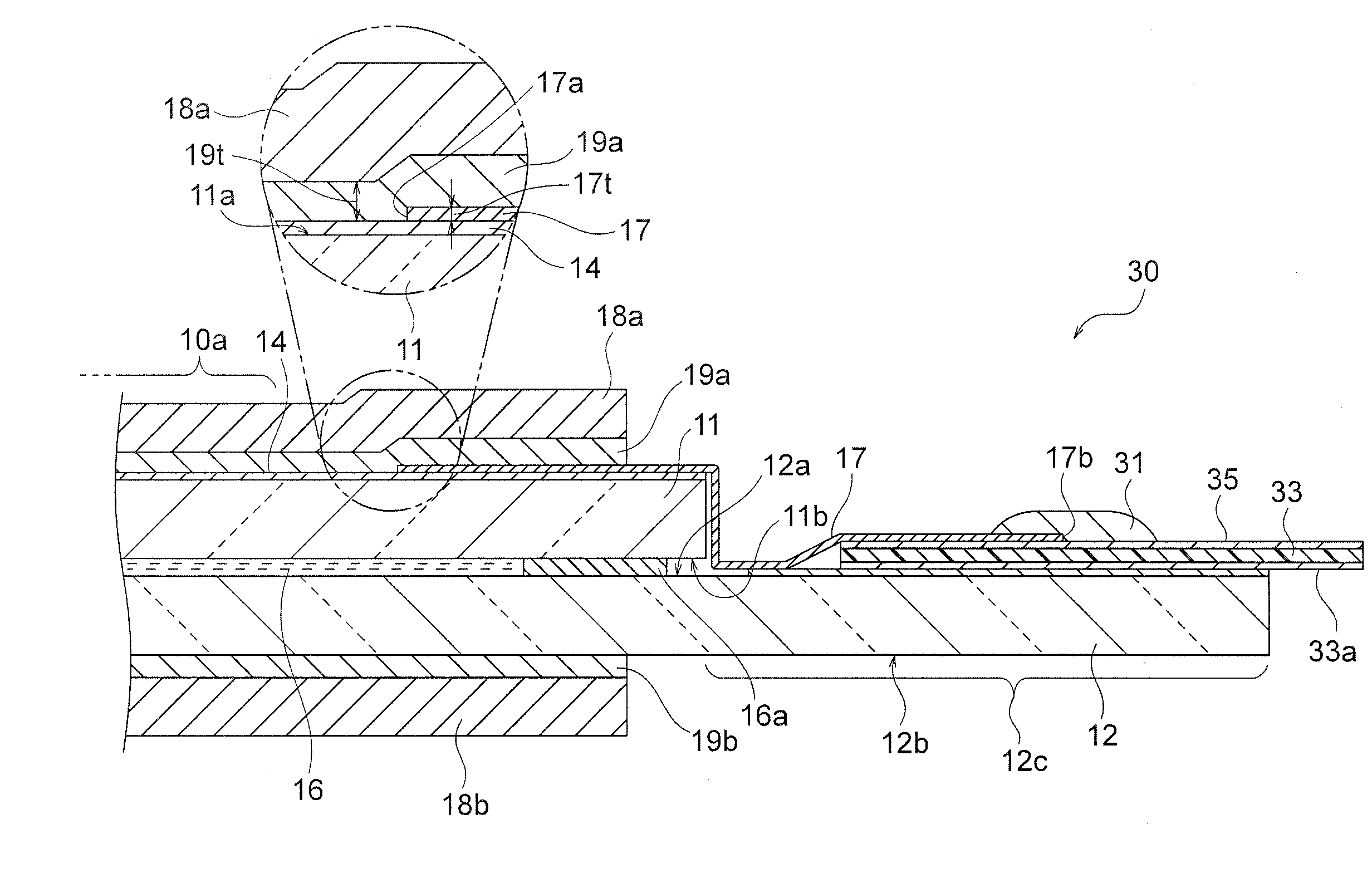
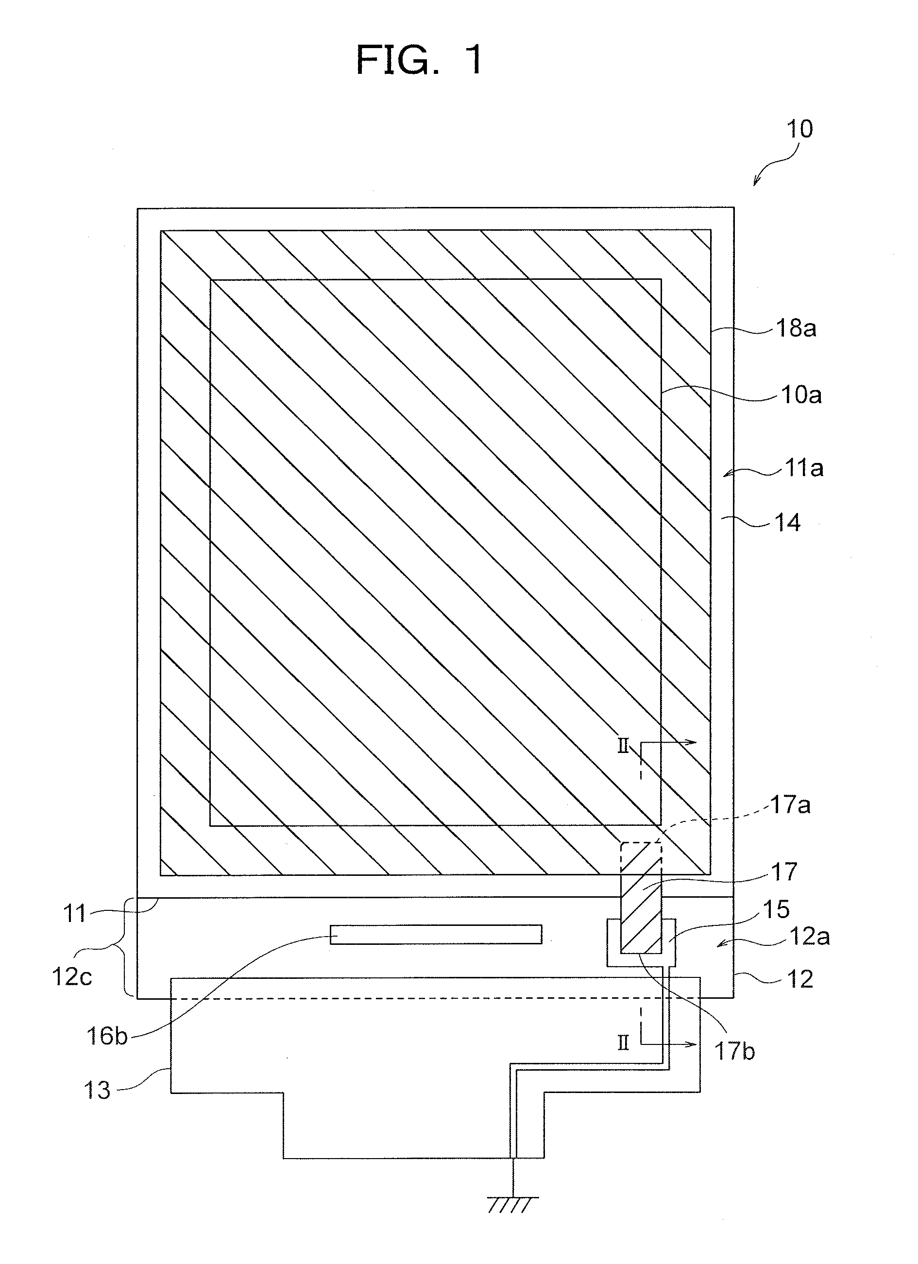
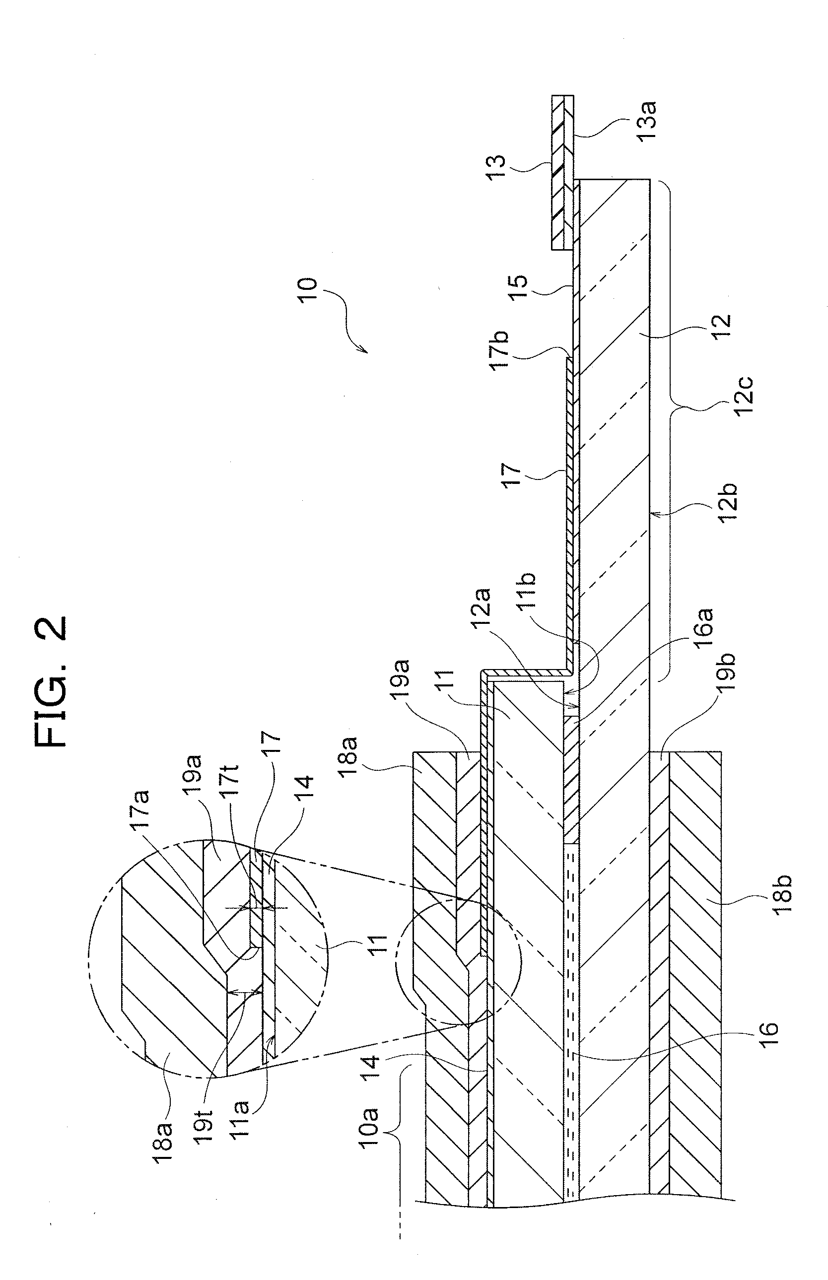
[0044]FIG. 1 is a plan view showing a liquid crystal display device according to a first exemplary embodiment. FIG. 2 is a sectional view taken along a line II-II of FIG. 1. In FIG. 1, oblique lines are applied to the surfaces of a polarization plate 18a and a conductive tape 17 for clarity. In FIG. 2, a part of the drawing is surrounded by a circle with an alternate short and long dash line and shown as an enlarged view. Hereinafter, explanations will be provided by referring to FIG. 1 and FIG. 2.
[0045]A CF glass substrate 11, an ITO layer 14, and a polarization plate 18a of the first exemplary embodiment are examples of “substrate”, “transparent conductive layer”, and “polarization plate” in a conductive tape attaching structure of a liquid crystal display device in the scope of the appended claims, respectively. The CF glass substrate 11, a TFT glass substrate 12, an FPC substrate 13, the ITO layer 14, the polarization plate 18a, and a polarization plate 18b of the first exemplar...
second exemplary embodiment
[0068]FIG. 3 is a sectional view showing a liquid crystal display device according to a second exemplary embodiment. In FIG. 3, shown are the sections that are different from those of the first exemplary embodiment and surroundings thereof. FIG. 3 corresponds to the sectional view taken along the line II-II of FIG. 1. Hereinafter, explanations will be provided by referring to FIG. 3.
[0069]In a liquid crystal display device 20 of the second exemplary embodiment, a resin 21 is applied on the other end 17b side of the conductive tape 17. That is, the conductive tape 17 is fixed to the TFT glass substrate 12 by the resin 21 applied from the above the conductive tape 17, and connected to the conductor pattern 15 by the conductive adhesive contained in the conductive tape 17.
[0070]As shown in FIG. 3, one end 17a side of the conductive tape 17 is fixed by overlapping and laminating the polarization plate 18a, and the other end 17b side of the conductive tape 17 is laminated to the conducto...
third exemplary embodiment
[0072]FIG. 4 is a sectional view showing a liquid crystal display device according to a third exemplary embodiment. In FIG. 4, shown are the sections that are different from those of the first exemplary embodiment and surroundings thereof. FIG. 4 corresponds to the sectional view taken along the line II-II of FIG. 1. Hereinafter, explanations will be provided by referring to FIG. 4.
[0073]An FPC substrate 33 of the third exemplary embodiment is an example of “third substrate” in the liquid crystal display device in the scope of the appended claims.
[0074]A liquid crystal display device 30 of the third exemplary embodiment further includes the FPC substrate 33 which includes a conductor pattern 35 and is provided on the TFT glass substrate 12. The conductive tape 17 is fixed to the FPC substrate 33 by soldering and connected to the conductor pattern 35 by a conductive adhesive contained in the conductive tape 17. That is, the other end 17b of the conductive tape 17 is covered by the so...
PUM
| Property | Measurement | Unit |
|---|---|---|
| Thickness | aaaaa | aaaaa |
| Size | aaaaa | aaaaa |
| Electrical conductor | aaaaa | aaaaa |
Abstract
Description
Claims
Application Information
 - Generate Ideas
- Intellectual Property
- Life Sciences
- Materials
- Tech Scout
- Unparalleled Data Quality
- Higher Quality Content
- 60% Fewer Hallucinations
Browse by: Latest US Patents, China's latest patents, Technical Efficacy Thesaurus, Application Domain, Technology Topic, Popular Technical Reports.
© 2025 PatSnap. All rights reserved.Legal|Privacy policy|Modern Slavery Act Transparency Statement|Sitemap|About US| Contact US: help@patsnap.com