Light-emitting apparatus

a technology of light-emitting apparatus and light-emitting device, which is applied in the direction of lighting and heating apparatus, semiconductor devices for light sources, and semiconductor/solid-state device details. it can solve the problems of decrease in emission output, and inability to realize high-power leds. it increases the amount of light, and reduces the loss of emitted light

Active Publication Date: 2016-01-14
NICHIA CORP
View PDF0 Cites 3 Cited by
  • Summary
  • Abstract
  • Description
  • Claims
  • Application Information

AI Technical Summary

Benefits of technology

[0021]In the light-emitting apparatus according to the present invention, the light-reflecting layer reflects light emitted by the semiconductor device toward a lower position (toward the substrate), thereby enabling effective use of the emitted light with a reduction in loss of the emitted light. This makes it possible to increase the amount of light that is emitted by the light-emitting apparatus. Further, since the light-reflecting layer is covered with the covering layer, the light-emitting apparatus inhibits the light-reflecting layer from being altered or deteriorating. Furthermore, the light-emitting apparatus inhibits a decrease in reflectance from being caused by the alteration or deterioration.
[0022]Further, the light-emitting apparatus according to the present invention sufficiently protects the light-reflecting layer by the covering layer, thus making it possible to apply dimethyl silicone or methyl rubber as the sealing resin. Dimethyl silicone and methyl rubber are somewhat lower in gas sealing properties in some cases, but exhibit high heat resistance and a high degree of adhesion to glass.
[0023]In the method according to the present invention for manufacturing a package for a light-emitting apparatus, at the same time as a substrate material obtained by stacking green sheets is fired, a reflecting layer and a covering layer covering the reflecting layer are fired, whereby a package for a light-emitting apparatus is manufactured. This makes it unnecessary to execute more than one firing step, thus achieving a low cost.

Problems solved by technology

However, the conventional arrangements cause the following problems.
Depending on the material, the LTCC substrate transmits or absorbs light emitted by an LED chip, thereby causing a decrease in emission output.
However, the conventional arrangements of Patent Literatures 1 and 2 take no measures against light reflection or light transmission on a surface of an LTCC substrate.
Further, since the conventional arrangements are each structured to have a step beside a surface on which an LED chip is mounted, thus causing a loss in emitted light.
Therefore, the conventional arrangements are not arranged to realize a high-power LED.
Further, in the arrangement of Non Patent Literature 1, unfortunately, the metal reflecting layer is altered or deteriorates, for example, due to external moisture or oxygen and further decreases in reflectance due to the alteration or deterioration.

Method used


Image

  • Light-emitting apparatus
  • Light-emitting apparatus
  • Light-emitting apparatus

Examples


embodiment 1

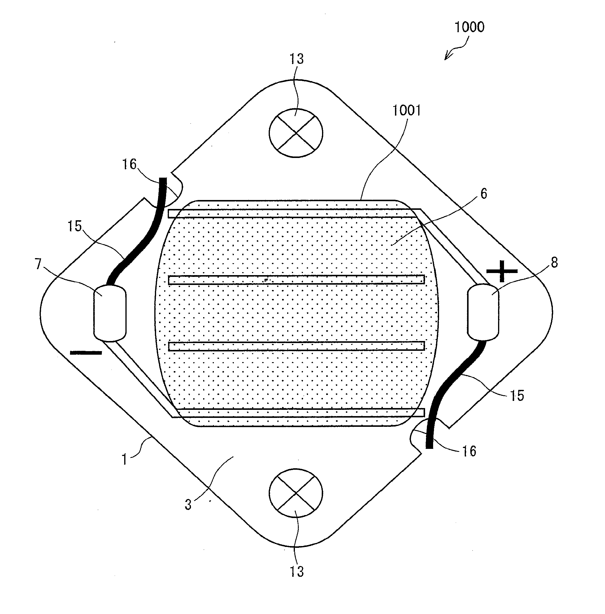
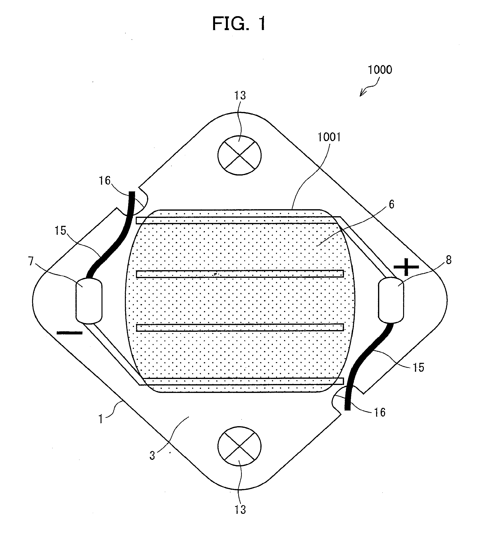
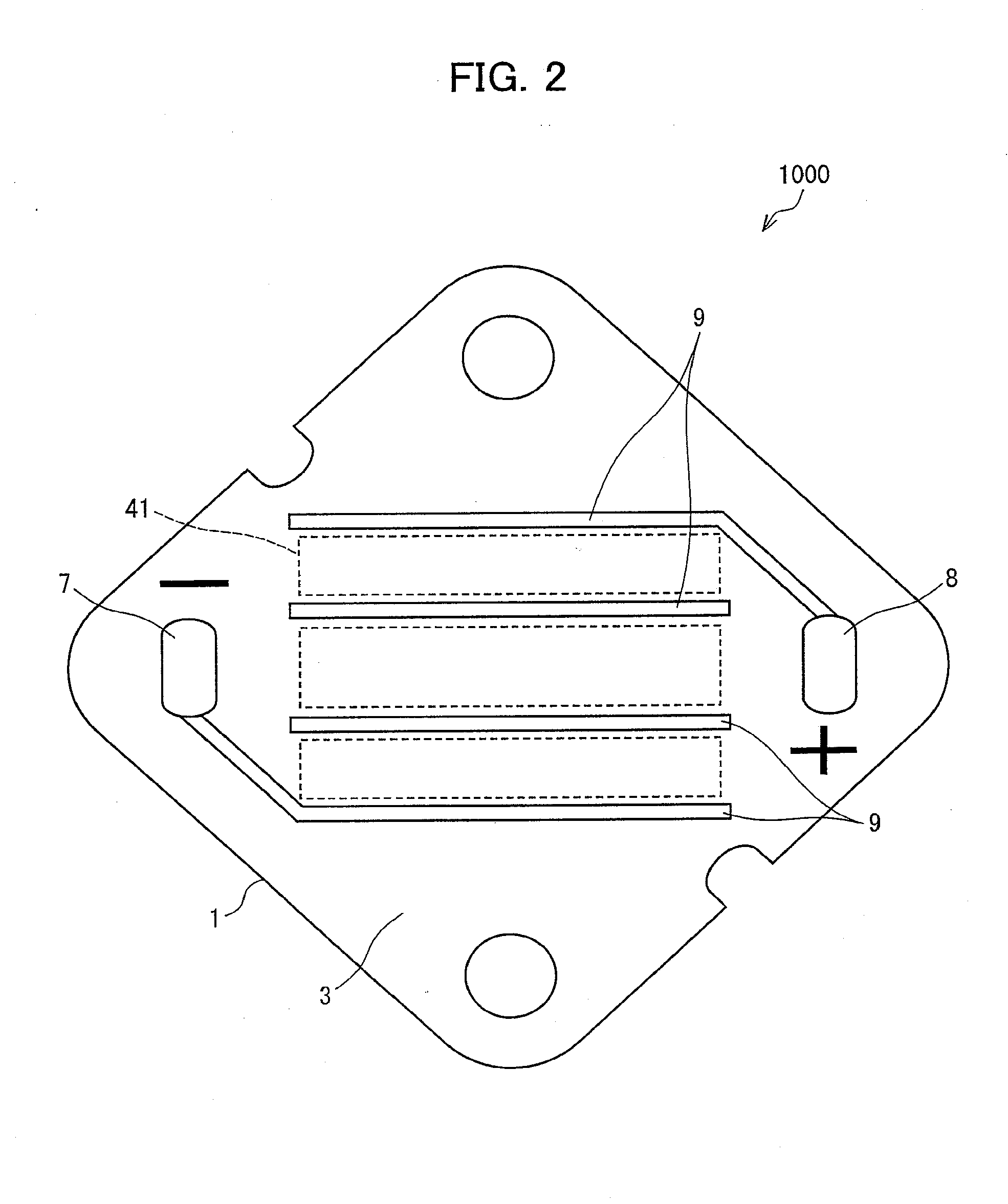
[0069]FIG. 7(a) is a cross-sectional view schematically illustrating a light-emitting apparatus 1002 according to another embodiment of the present invention, and FIG. 7(b) is a plan view illustrating the light-emitting apparatus 1002. For convenience of explanation, members having the same functions as those used in Embodiment 1 are given the same reference numerals, and will not be described below. The light-emitting apparatus 1002 includes: a low temperature co-fired ceramic (LTCC) substrate 10; a silver reflecting layer 2 formed on the LTCC substrate 10; a glass layer 3 covering the silver reflecting layer 2; LED chips 4 placed on the glass layer 3; and positive and negative electrode external connection terminals 81 and 71 formed on the glass layer 3. The LED chips 4 are electrically connected to each of the external connection terminals 81 and 71 via bonding wires W. The LED chips 4 and the bonding wires W are sealed with a domed luminescent material-containing sealing resin 6...

embodiment 2

[0085]FIG. 9 is a cross-sectional view schematically illustrating a light-emitting apparatus 1003 according to another embodiment of the present invention. For convenience of explanation, members having the same functions as those used in Embodiment 2 are given the same reference numerals, and will not be described below. The light-emitting apparatus 1003 includes: a low temperature co-fired ceramic (LTCC) substrate 11; a silver reflecting layer 2 formed on the LTCC substrate 11; a glass layer 3 covering only the silver reflecting layer 2 on the LTCC substrate 11; LED chips 4 placed on the glass layer 3; and positive and negative electrode external connection terminals 81 and 71 formed on the LTCC substrate 11. The LED chips 4 are electrically connected to each of the external connection terminals 81 and 71 via bonding wires W. The LED chips 4, the external connection terminals 81 and 71, and the bonding wires W are sealed with a luminescent material-containing sealing resin 62. The...

embodiment 4

[0096]FIG. 10 is a cross-sectional view schematically illustrating a light-emitting apparatus 1004 according to another embodiment of the present invention. For convenience of explanation, members having the same functions as those used in Embodiment 4 are given the same reference numerals, and will not be described below. The light-emitting apparatus 1004 includes: an alumina substrate 12; a silver reflecting layer 2 formed on the alumina substrate 12; a glass layer 3 covering only the silver reflecting layer 2; LED chips 4 placed on the glass layer 3; and positive and negative electrode external connection terminals 81 and 71 formed on the alumina substrate 12. The LED chips 4 are electrically connected to each of the external connection terminals 81 and 71 via bonding wires W. The LED chips 4, the bonding wires W, and the external connection terminals 81 and 71 are sealed with a luminescent material-containing sealing resin 62; however, the luminescent material-containing sealing...


PUM


Abstract

A light-emitting apparatus of the present invention has (i) a semiconductor device which emits light toward a higher position than a substrate and (ii) a plurality of external connection terminals, and includes: a light-reflecting layer, provided on the substrate, which reflects the light emitted by the semiconductor device; and a covering layer which covers at least the light-reflecting layer and which transmits the light reflected by the light-reflecting layer. Further, the semiconductor device is provided on the covering layer, and is electrically connected to the external connection terminals via connecting portions, and the semiconductor device and the connecting portions are sealed with a sealing resin so as to be covered. Therefore, the light-emitting apparatus has increased efficiency with which light is taken out, and can prevent a reflecting layer from being altered, deteriorating, and decreasing in reflectance.

Description

CROSS-REFERENCE TO RELATED APPLICATIONS[0001]This application is a continuation application of U.S. application Ser. No. 14 / 467,836, filed Aug. 25, 2014, which is a continuation application of U.S. application Ser. No. 14 / 105,638, filed on Dec. 13, 2013, now U.S. Pat. No. 8,835,970, which is a divisional application of U.S. application Ser. No. 12 / 490,192, filed Jun. 23, 2009, now U.S. Pat. No. 8,680,546, which claims priority under 35 U.S.C. §119(a) to Patent Application No. 2008-164910 filed in Japan on Jun. 24, 2008, and Patent Application No. 2008-269858 filed in Japan on Oct. 20, 2008, the entire contents of which are hereby incorporated by reference.FIELD OF THE INVENTION[0002]The present invention relates light-emitting apparatuses each including a light-emitting diode (LED) chip and a reflecting layer for efficiently taking out light emitted by the LED. In particular, the present invention relates to a light-emitting apparatus that prevents the reflecting layer from being al...

Claims


Application Information

Patent Timeline
Patent Type & Authority Applications(United States)
IPC IPC(8): H01L33/62F21V9/40H01L23/12H01L23/13H01L33/32H01L33/48H01L33/50H01L33/54H01L33/56H01L33/60
CPCH01L33/50H01L33/62H01L24/97H01L25/0753H01L2224/48091H01L2224/48227H01L2224/48228H01L2224/97H01L2924/01012H01L2924/01013H01L2924/0102H01L2924/0103H01L2924/01038H01L2924/01047H01L2924/01056H01L2924/01058H01L2924/01063H01L2924/01078H01L2924/01079H01L2924/09701H01L2924/19107H01L2924/01005H01L2924/01006H01L2924/01024H01L2924/01033H01L2924/0104H01L2924/01074H01L33/46H01L2924/12041H01L2224/73265H01L2224/49113H01L2924/15787H01L2924/15788H01L2924/181F21K9/23F21Y2115/10H01L33/60H01L33/56H01L2224/85H01L2924/00014H01L2924/00H01L2924/00012H01L33/641H01L2933/0066
Inventor KONISHI, MASAHIROKONDO, MASAKIHORIO, TAKAAKIMATSUO, TAKANOBUHATA, TOSHIOOHTA, KIYOHISA
Owner NICHIA CORP
Why Eureka
Try Eureka