Method for producing electronic component, bump-formed plate-like member, electronic component, and method for producing bump-formed plate-like member
- Summary
- Abstract
- Description
- Claims
- Application Information
AI Technical Summary
Benefits of technology
Problems solved by technology
Method used
Image

Examples
example 1
[0056]In the present example, an example of a “bump-formed plate-like member having a deformable portion” according to the present invention, an example of an electronic component according to the present invention, using the bump-formed plate-like member having a deformable portion, and an example of a method for producing an electronic component, using transfer molding are described.
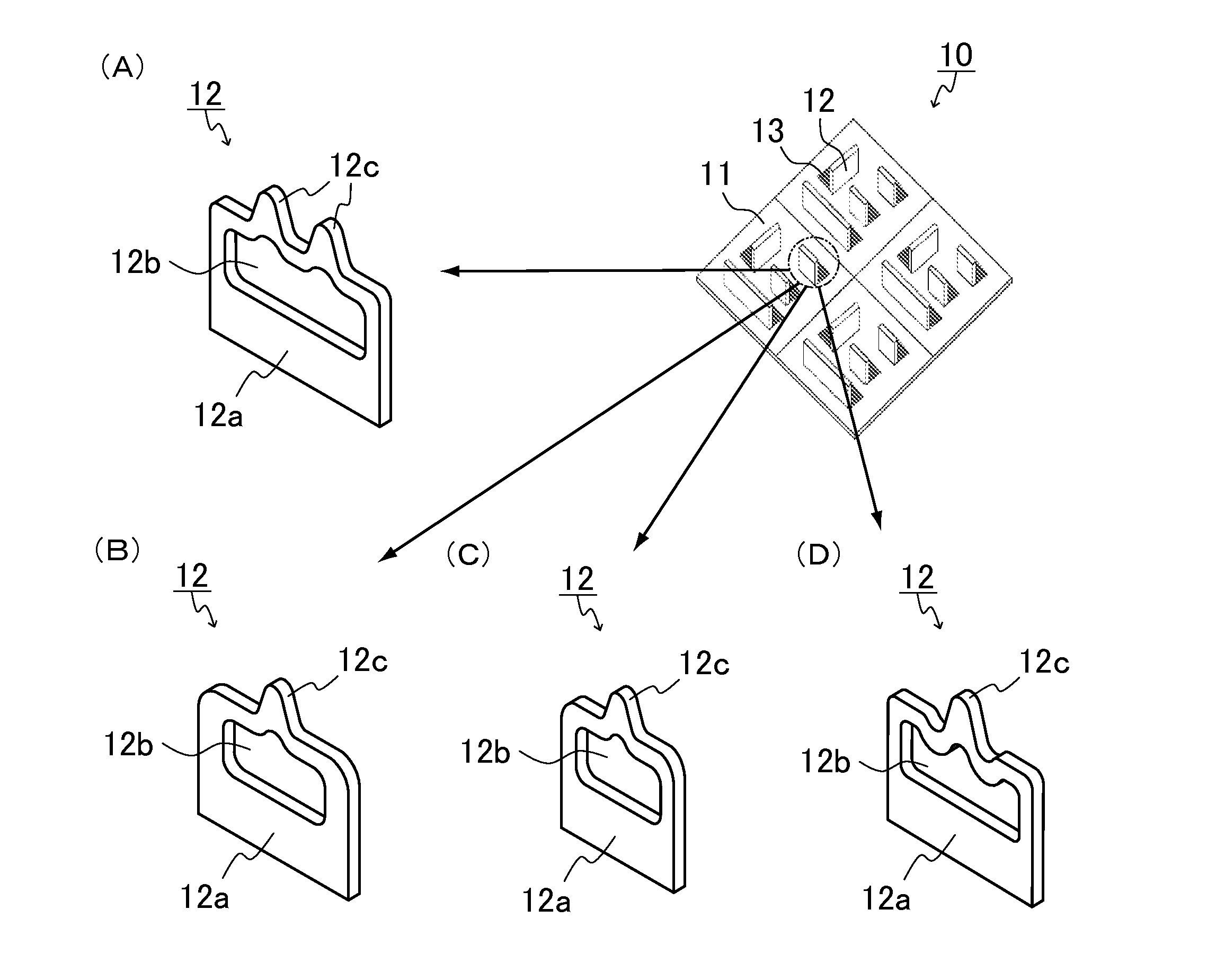
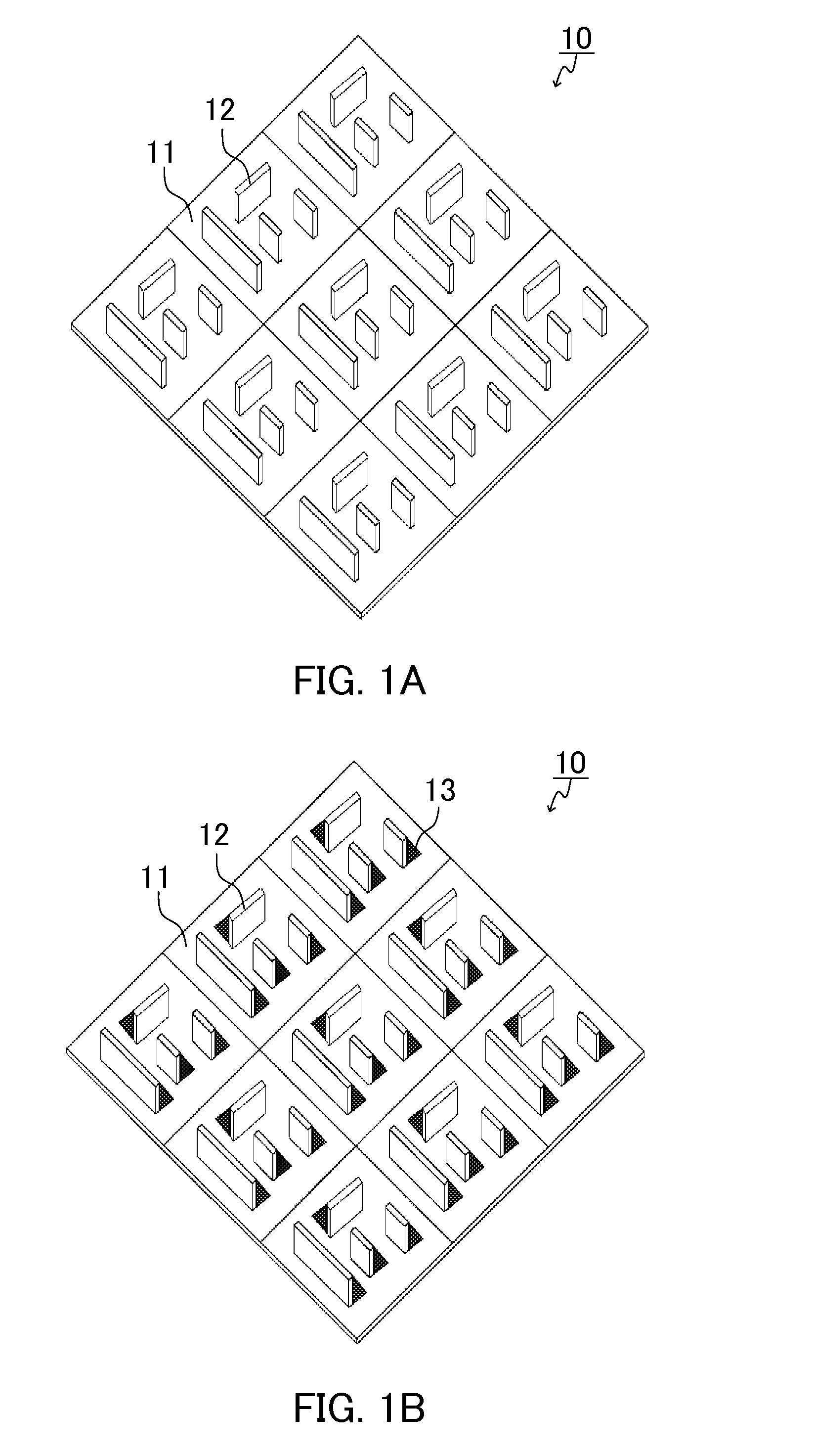
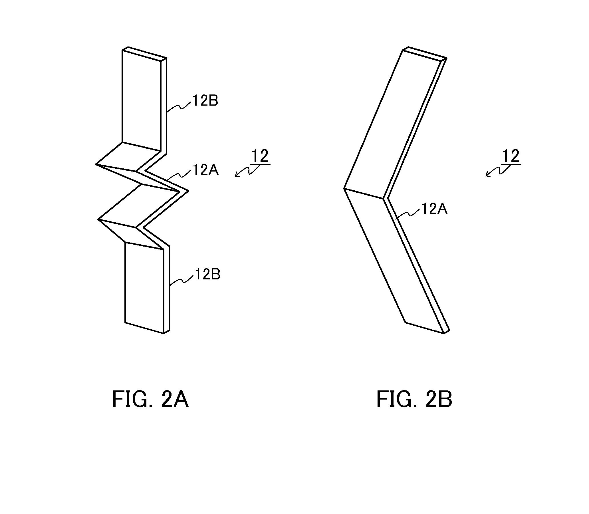
[0057]A structure of the bump-formed plate-like member having a deformable portion according to the present example is schematically shown in perspective views of FIGS. 1A and 1B. As shown in FIGS. 1A and 1B, this bump-formed plate-like member 10 having a deformable portion is formed by forming a pattern of a bump(s) 12 having a deformable portion on a plate-like member 11. Although the length (height) of the bump(s) 12 is not limited to particular lengths, the length can be set appropriately according to the thickness of a completed electronic component (molded package), for example. In the present in...
example 2
[0090]In FIGS. 7 to 10, another example of the present invention is described with reference to FIGS. 7 to 10. In the present example, an example of a method for producing an electronic component using compression molding is described. Each of bumps of a bump-formed plate-like member used in the present example has a deformable portion.
[0091]First, a compression molding device (a device for producing an electronic component) is provided. The step cross-sectional view of FIG. 7 shows the structure of a part of a molding die that is a part of the compression molding device. As shown in FIG. 7, this compression molding device includes, as main components, an upper die 101, a lower die 111, and an intermediate die (intermediate plate) 102. The lower die 111 includes a lower die cavity bottom member 111a and lower-die peripheral members (main body of the lower die) 112 and 113. The lower-die peripheral members (main body of the lower die) 112 and 113 are frame-shaped lower die cavity sid...
example 3
[0110]Yet another example of the present invention is described below. The present example shows yet another example of the production method using compression molding which uses a bump-formed plate-like member having a deformable portion.
[0111]The production method of the present example is schematically shown in step cross-sectional views of FIGS. 13 to 16. As shown in FIGS. 13 to 16, the present example is different from Example 2 (FIGS. 7 to 10) in that a release film 100 is not used, and the shape of a plate-like member 11 is different.
[0112]In the present example, the outer edge of the plate-like member 11 has a protuberance, so that the central portion of the plate-like member 11 becomes a resin containing portion. More specifically, as shown in FIGS. 11 to 14, the outer edge of the plate-like member 11 has a protuberance on the bump 12-formed surface of the plate-like member 11, so that a wall-like member 11b is formed. Thus, the resin containing portion 11c is formed in the...
PUM
| Property | Measurement | Unit |
|---|---|---|
| Current | aaaaa | aaaaa |
| Time | aaaaa | aaaaa |
| Pressure | aaaaa | aaaaa |
Abstract
Description
Claims
Application Information
 - Generate Ideas
- Intellectual Property
- Life Sciences
- Materials
- Tech Scout
- Unparalleled Data Quality
- Higher Quality Content
- 60% Fewer Hallucinations
Browse by: Latest US Patents, China's latest patents, Technical Efficacy Thesaurus, Application Domain, Technology Topic, Popular Technical Reports.
© 2025 PatSnap. All rights reserved.Legal|Privacy policy|Modern Slavery Act Transparency Statement|Sitemap|About US| Contact US: help@patsnap.com