Display device and drive current detection method for same

a technology of drive current and display device, which is applied in the field of display devices, can solve problems such as degrading display quality, and achieve the effects of high accuracy, high accuracy and high accuracy

Active Publication Date: 2016-02-25
SHARP KK
View PDF32 Cites 61 Cited by
  • Summary
  • Abstract
  • Description
  • Claims
  • Application Information

AI Technical Summary

Benefits of technology

[0039]According to the first or nineteenth aspect of the present invention, by suitably controlling the reference voltage, even when the threshold voltage of the drive transistor is changed, a change in the amount of drive current flowing through the drive transistor is suppressed, enabling to detect the drive current with a high accuracy. In addition, upon current detection, a change in the end-to-end voltage of the electro-optical element is suppressed to prevent an unwanted current from flowing through the electro-optical element. By this, the drive current can be detected with a high accuracy.
[0040]According to the second aspect of the present invention, by suitably controlling the reference voltage by controlling the reference voltage based on data according to the threshold voltage of the drive transistor, which is stored for each pixel circuit, the drive current can be detected with a high accuracy.
[0041]According to the third aspect of the present invention, by suitably controlling the reference voltage by controlling the reference voltage based on a statistical value of the threshold voltages of the drive transistors, the drive current can be detected with a high accuracy.
[0042]According to the fourth aspect of the present invention, by storing data representing a difference between the statistical value of the threshold voltages of the drive transistors and the reference voltage, the number of bits of data to be stored is reduced, enabling to reduce the capacity of the storage unit.
[0043]According to the fifth aspect of the present invention, data according to the threshold voltages of the drive transistors can be obtained based on the results of drive current detection.
[0044]According to the sixth aspect of the present invention, by compensating for the threshold voltage and gain of the drive transistor on a per pixel circuit basis, the image quality of a display image can be improved.

Problems solved by technology

Due to this, variations also occur in the luminance of pixels, degrading display quality.

Method used


Image

  • Display device and drive current detection method for same
  • Display device and drive current detection method for same
  • Display device and drive current detection method for same

Examples


first embodiment

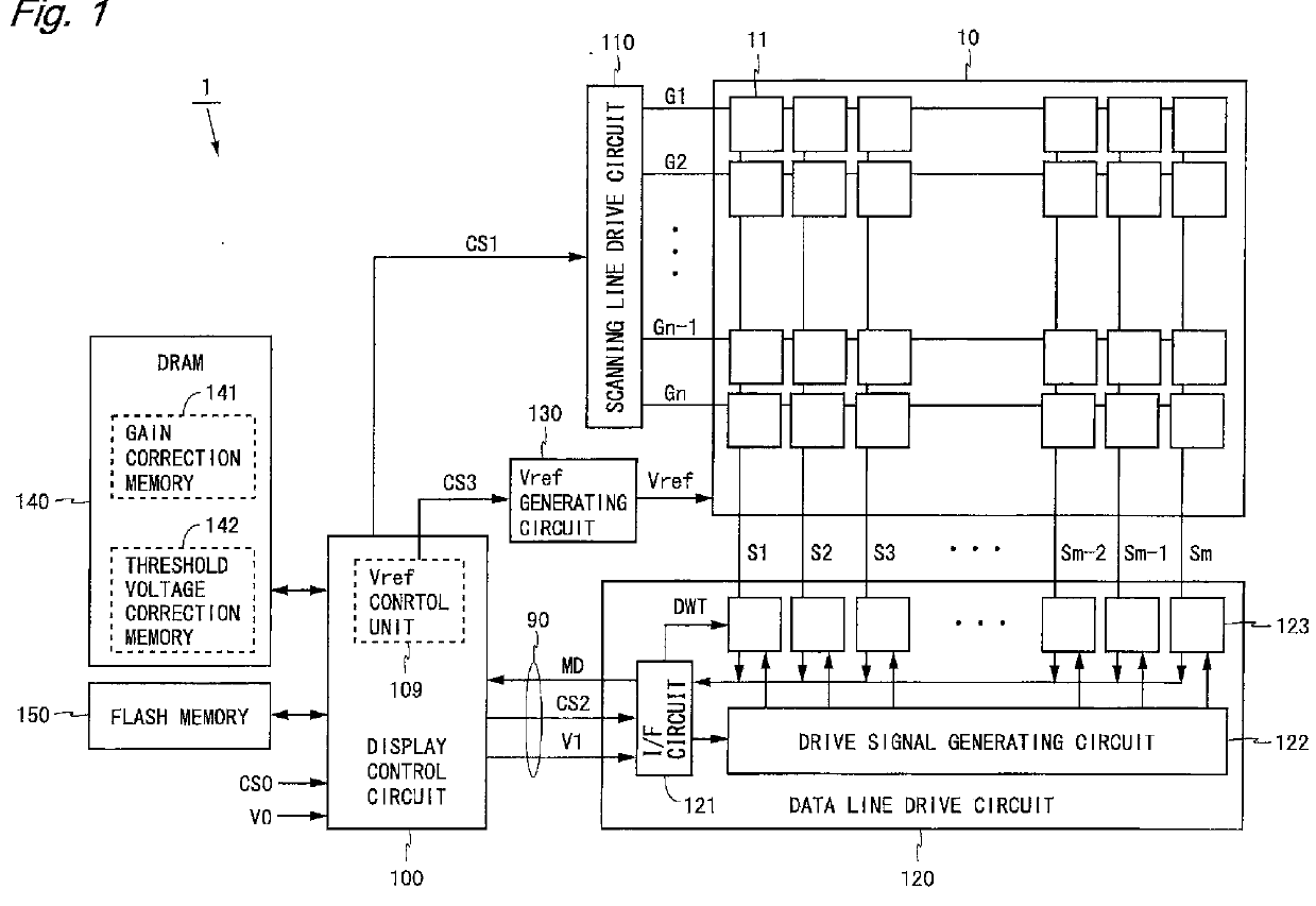
[0089]FIG. 1 is a block diagram showing a configuration of an organic EL display device according to a first embodiment of the present invention. An organic EL display device 1 shown in FIG. 1 includes a display unit 10, a display control circuit 100, a scanning line drive circuit 110, a data line drive circuit 120, a Vref generating circuit 130, a DRAM 140, and a flash memory 150. The organic EL display device 1 is an active matrix-type display device.

[0090]The display unit 10 includes n scanning lines G1 to Gn, m data lines S1 to Sm, and (m×n) pixel circuits 11. The data lines S1 to Sm are arranged parallel to each other. The scanning lines G1 to Gn are arranged parallel to each other and orthogonal to the data lines S1 to Sm. The scanning lines G1 to Gn intersect with the data lines S1 to Sm at (m×n) locations. The (m×n) pixel circuits 11 are provided at the respective intersections of the scanning lines G1 to Gn and the data lines S1 to Sm. A direction in which the scanning line...

second embodiment

[0163]FIG. 15 is a block diagram showing a configuration of an organic EL display device according to a second embodiment of the present invention. An organic EL display device 2 shown in FIG. 15 includes a display unit 10, a display control circuit 200, a scanning line drive circuit 210, a data line drive circuit 220, and a Vref generating circuit 130. In the following, of the components of embodiments, the same components as those of the previously described embodiment are denoted by the same reference characters and description thereof is omitted.

[0164]As with the display control circuit 100 according to the first embodiment, the display control circuit 200 controls the scanning line drive circuit 210 and the data line drive circuit 220. In the organic EL display device 2, video data V1 may be the same as video data V0 or may be one obtained by performing a correction process, etc., on video data V0. The scanning line drive circuit 210 drives scanning lines G1 to Gn at different ...

third embodiment

[0197]FIG. 22 is a block diagram showing a configuration of an organic EL display device according to a third embodiment of the present invention. An organic EL display device 3 shown in FIG. 22 includes a display unit 13, a display control circuit 300, a scanning line drive circuit 210, a data line drive circuit 320, and a Vref generating circuit 130.

[0198]The display unit 13 is such that a characteristic detection transistor 14 is added to the display unit 10 according to the first embodiment. The data line drive circuit 320 is such that a characteristic detection circuit 321 is added to the data line drive circuit 220 according to the second embodiment. The characteristic detection circuit 321 is connected to the characteristic detection transistor 14 and detects a characteristic (e.g., threshold voltage) of the characteristic detection transistor 14. The data line drive circuit 320 outputs, to the display control circuit 300, characteristic data CD representing the characteristi...


PUM


Abstract

A data line drive circuit provides a voltage according to a detection voltage and to a reference voltage, between the gate and source of a drive transistor in a pixel circuit, and detects a drive current having passed through the drive transistor and outputted external to the pixel circuit. A threshold voltage correction memory stores, for each pixel circuit, data representing a threshold voltage of the drive transistor. A display control circuit controls the reference voltage based on the data stored in the threshold voltage correction memory. By this, even if the threshold voltage of the drive transistor is changed, the drive current can be detected with a high accuracy. The threshold voltage correction memory may store, for each pixel circuit, data representing a difference between the threshold voltage of the drive transistor and the reference voltage.

Description

TECHNICAL FIELD[0001]The present invention relates to a display device, and more particularly to a display device having pixel circuits each including an electro-optical element such as an organic EL (Electro Luminescence) element, and a drive current detection method for the display device.BACKGROUND ART[0002]For a slim, high image quality, and low power consumption display device, an organic EL display device is known. An active matrix-type organic EL display device has a plurality of two-dimensionally arranged pixel circuits each including an organic EL element and a drive transistor. The organic EL element is a self-light emitting type electro-optical element that changes in luminance according to a drive current. The drive transistor is provided in series with the organic EL element, and controls the amount of drive current flowing through the organic EL element, according to a gate-source voltage thereof.[0003]In general, a thin film transistor (hereinafter, abbreviated as TFT...

Claims


Application Information

Patent Timeline
Patent Type & Authority Applications(United States)
IPC IPC(8): G09G3/30
CPCG09G3/30G09G2330/028G09G2330/027G09G2300/0426G09G2310/0202G09G2310/0275G09G2330/021G09G3/3241G09G3/3266G09G2310/0251G09G2320/0285G09G2320/045G09G2330/12
Inventor KISHI, NORITAKAKATSUI, HIROMITSUNOGUCHI, NOBORUOHARA, MASANORIYAMANAKA, SHIGETSUGUOHTA, YOSHIFUMI
Owner SHARP KK
Why Eureka
Try Eureka