Circuit and method for adjusting select gate voltage of non-volatile memory
- Summary
- Abstract
- Description
- Claims
- Application Information
AI Technical Summary
Benefits of technology
Problems solved by technology
Method used
Image


Examples
Embodiment Construction
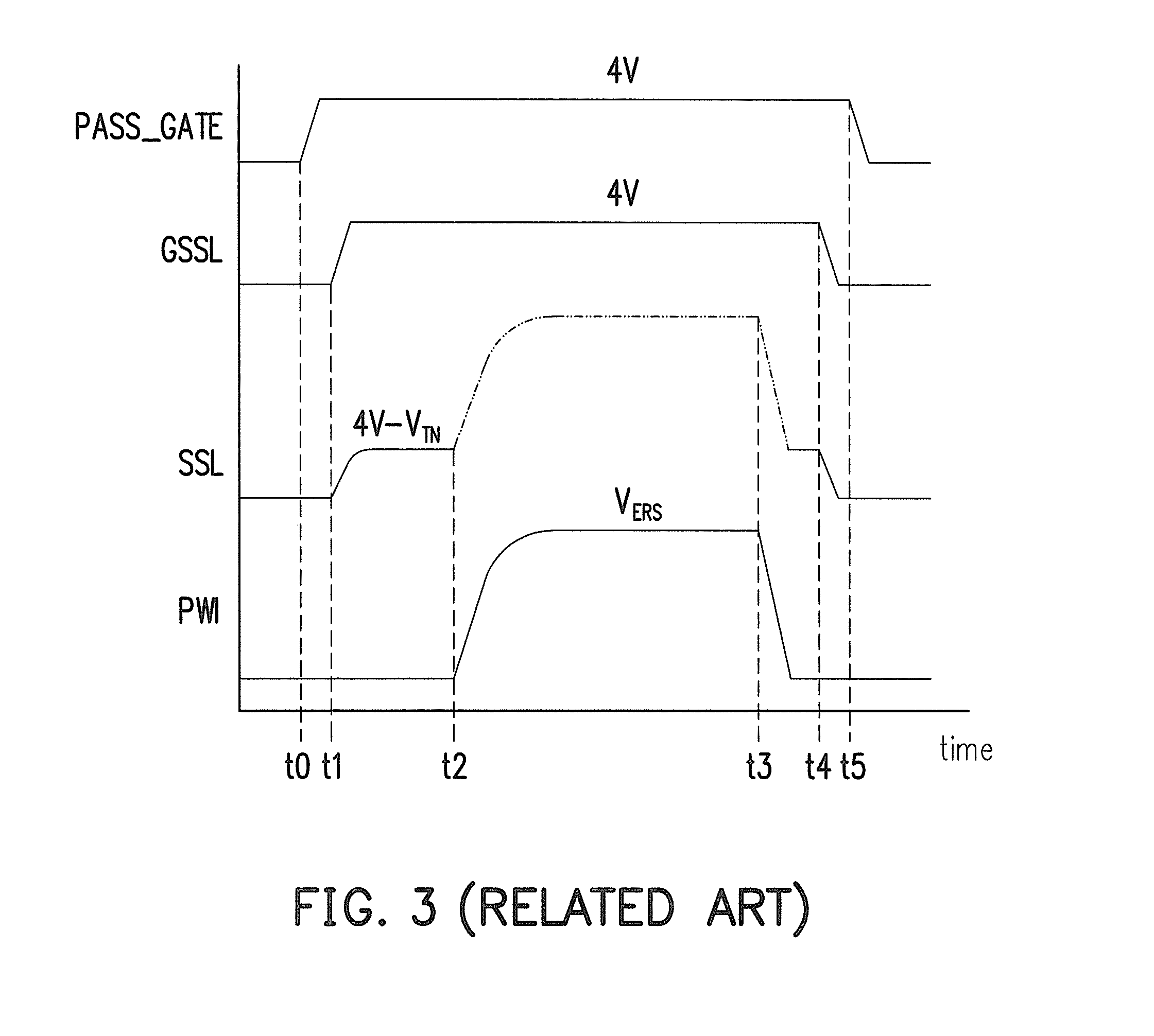
[0034]Reference will now be made in detail to the present embodiments of the invention, examples of which are illustrated in the accompanying drawings. Wherever possible, the same reference numbers are used in the drawings and the description to refer to the same or like parts.
[0035]FIG. 4 is a schematic diagram showing a circuit 400 for adjusting select gate voltage for an erase operation of a non-volatile memory according to an embodiment of the present invention. The circuit 400 includes a p-well PWI, a select gate SSL, a pass transistor 406, an adjustment unit 404, and switches 402 and 403. The pass transistor 406 is coupled to the select gate SSL. The adjustment unit 404 is coupled to the p-well PWI. The switch 402 is coupled between the pass transistor 406 and the adjustment unit 404. The switch 403 is coupled to the pass transistor 406.
[0036]In this embodiment, the non-volatile memory is a NAND flash memory. The select gate SSL and the p-well PWI is a part of a NAND string of...
PUM
 Abstract
Description
Claims
Application Information
 - R&D
- Intellectual Property
- Life Sciences
- Materials
- Tech Scout
- Unparalleled Data Quality
- Higher Quality Content
- 60% Fewer Hallucinations
Browse by: Latest US Patents, China's latest patents, Technical Efficacy Thesaurus, Application Domain, Technology Topic, Popular Technical Reports.
© 2025 PatSnap. All rights reserved.Legal|Privacy policy|Modern Slavery Act Transparency Statement|Sitemap|About US| Contact US: help@patsnap.com