Capacitor
a technology of capacitors and capacitors, applied in the field of capacitors, can solve the problems of difficult manufacturing of ceramics and inability to conduct electricity, and achieve the effects of maximizing capacitance, maximizing capacity, and effectively reducing manufacturing costs
- Summary
- Abstract
- Description
- Claims
- Application Information
AI Technical Summary
Benefits of technology
Problems solved by technology
Method used
Image
Examples
exemplary embodiment 1
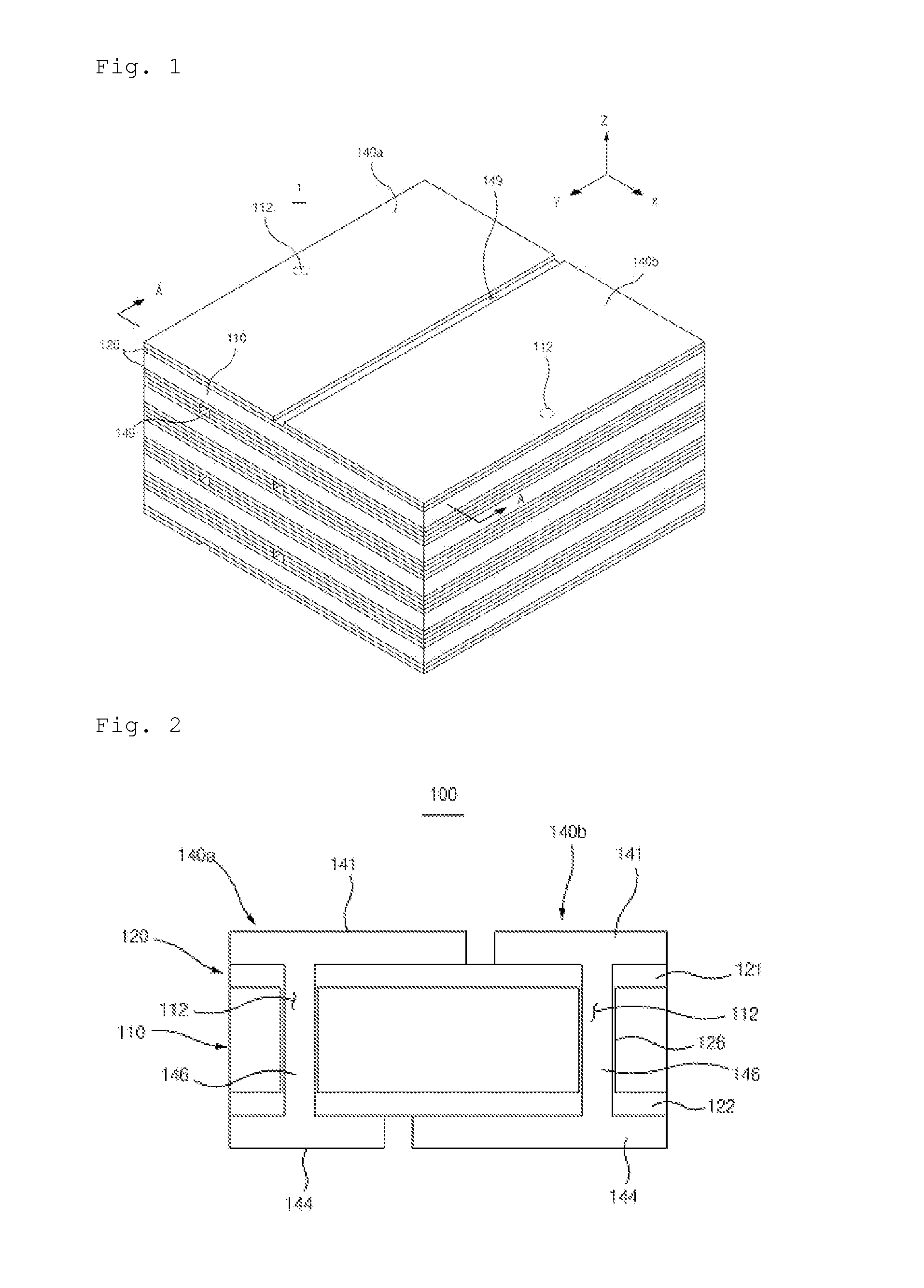
[0052]As illustrated in FIGS. 1 to 5, a capacitor 1 of the present exemplary embodiment includes a plurality of unit capacitors 100 sequentially stacked, each of the plurality of unit capacitors 100 including: a substrate 110; a dielectric layer 120 formed on the substrate 110; and an electrode layer comprising a first electrode layer 140a and a second electrode layer 140b formed on the dielectric layer 120, wherein the first electrode layer 140a and the second electrode layer 140b are separated from each other, the portion separating the first electrode layer 140a and the second electrode layer 140b is disposed on the upper side and the lower side of the substrate 110, and at least a portion of the first electrode layer 140a and at least a portion of the second electrode layer 140b are disposed on the same surface.
[0053]The substrate 110 is formed in the shape of a rectangular plate, and located in the center of the unit capacitor 100.
[0054]Although there is no material limitation ...
exemplary embodiment 2
[0087]The description of the elements identical to those of the above Exemplary Embodiment 1 will be omitted.
[0088]The unit capacitor 100′ of Exemplary Embodiment 2 has no hole in the substrate 110.
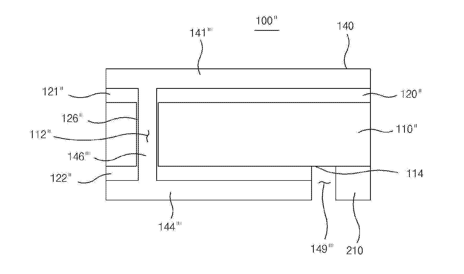
[0089]As illustrated in FIG. 6, the unit capacitor 100′ according to Exemplary Embodiment 2 includes: a side dielectric layer 126′ formed on the side surface of the substrate 110′ for connecting an upper dielectric layer 121′ and a lower dielectric layer 122′ along the side surface, wherein a side electrode layer 146′ is formed on the side dielectric layer 126′, and the upper electrode layer 141′ and the lower electrode layer 144′ are connected to the side electrode layer 146′.
[0090]The side dielectric layer 126′ is also an anodized layer formed by anodizing the substrate 110′ comprising aluminum.
[0091]The side dielectric layers 126′ are formed in the shape of a rectangle, and formed all over the right side surface and the left side surface of the substrate 110′ respectively.
[0092]And, th...
exemplary embodiment 3
[0094]The description of the elements identical to those of the above Exemplary Embodiments will be omitted.
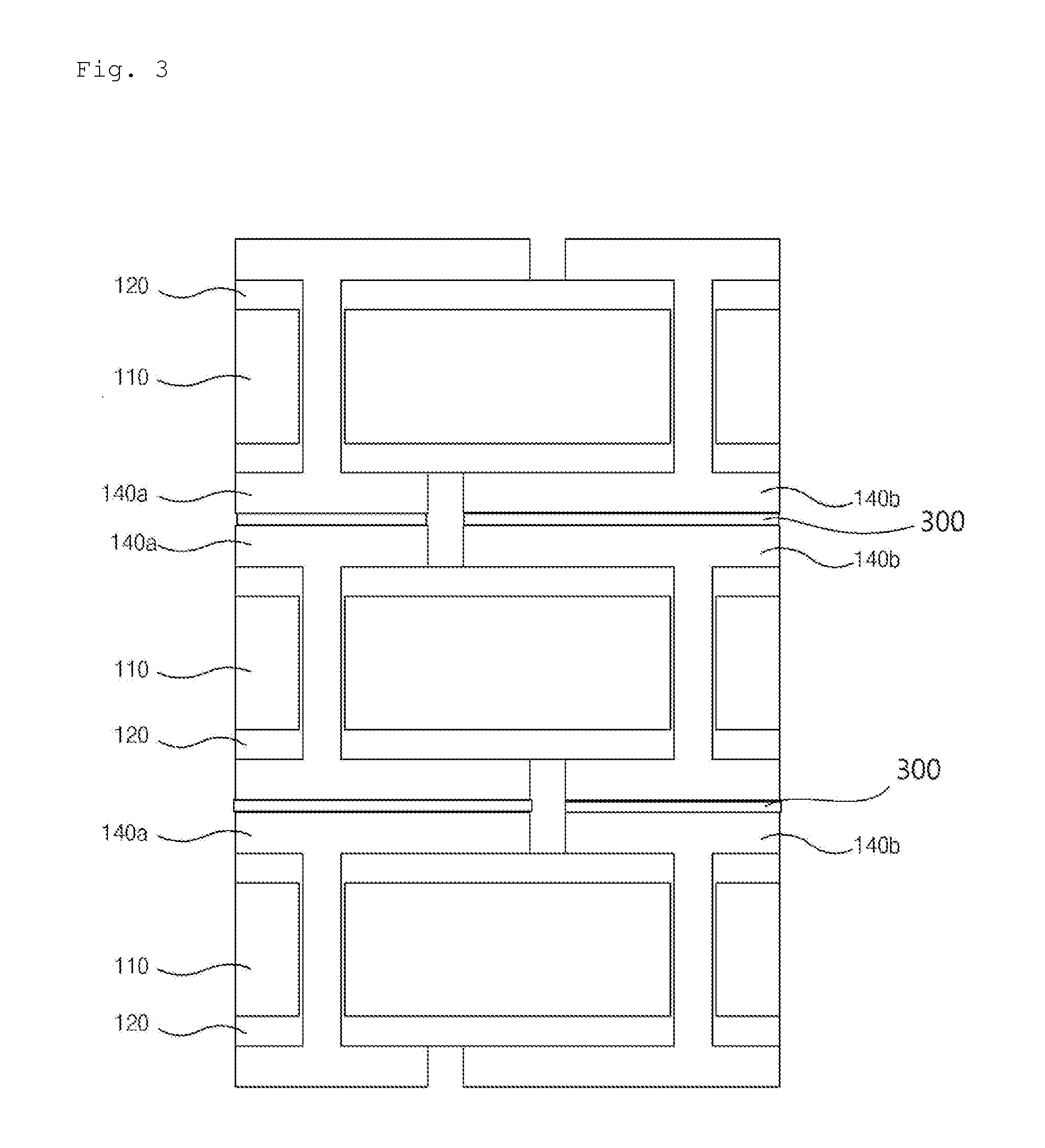
[0095]As illustrated in FIG. 7, a capacitor according to Exemplary Embodiment 3 includes unit capacitors 100′″, wherein each of the unit capacitors 100′″ includes: a dielectric layer; and a plurality of electrode layers comprising the first electrode layers 140a′, 140c, 140e, and 140g, and the second electrode layers 140b′, 140d, 140f, and 140h, wherein the first electrode layers 140a′, 140c, 140e, and 140g, and the second electrode layers 140b′, 140d, 140f, and 140h, are separated from each other, and at least a portion of the first electrode layers 140a′, 140c, 140e, and 140g, and at least a portion of the second electrode layers 140b′, 140d, 140f, and 140h are disposed on the same surface, and a plurality of the unit capacitors 100′″ are formed on a large single substrate 110′″ to be separated from each other.
[0096]The plurality of unit capacitors 100′″ can be formed to hav...
PUM
| Property | Measurement | Unit |
|---|---|---|
| height | aaaaa | aaaaa |
| areas | aaaaa | aaaaa |
| dielectric property | aaaaa | aaaaa |
Abstract
Description
Claims
Application Information


