

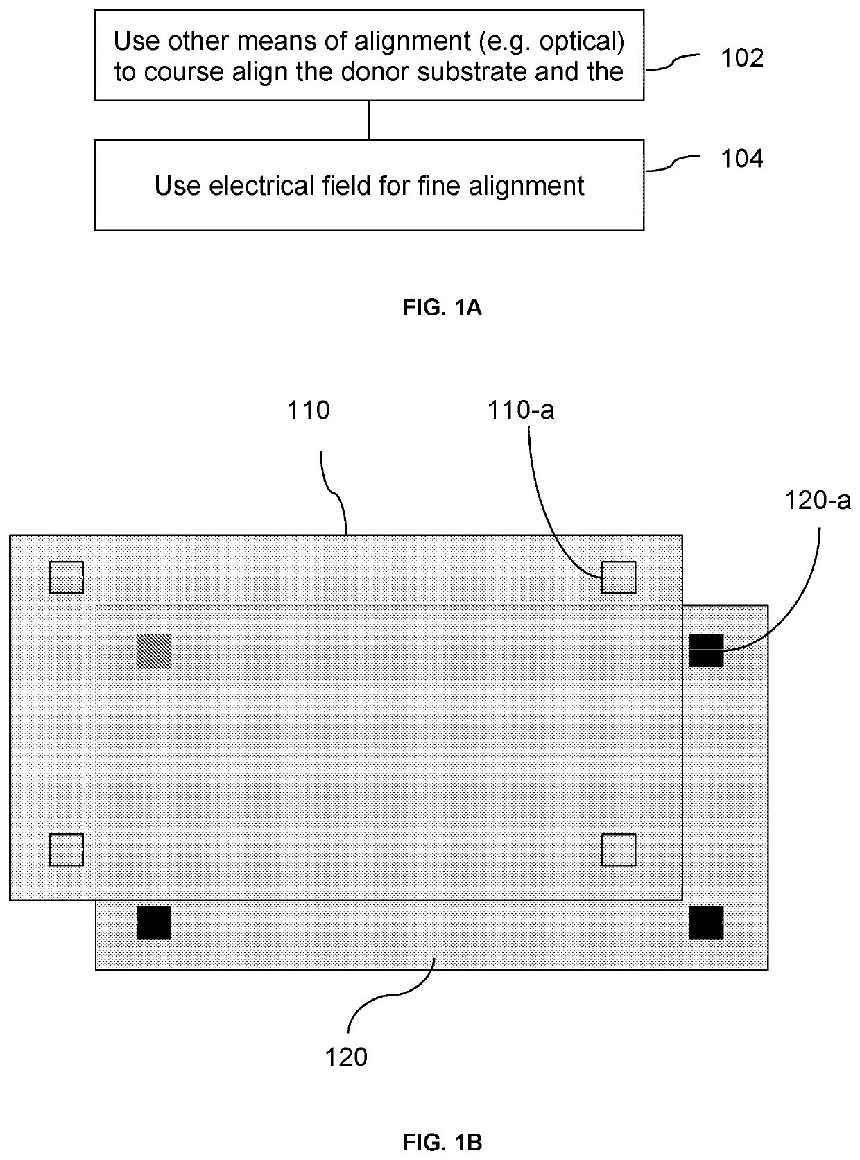
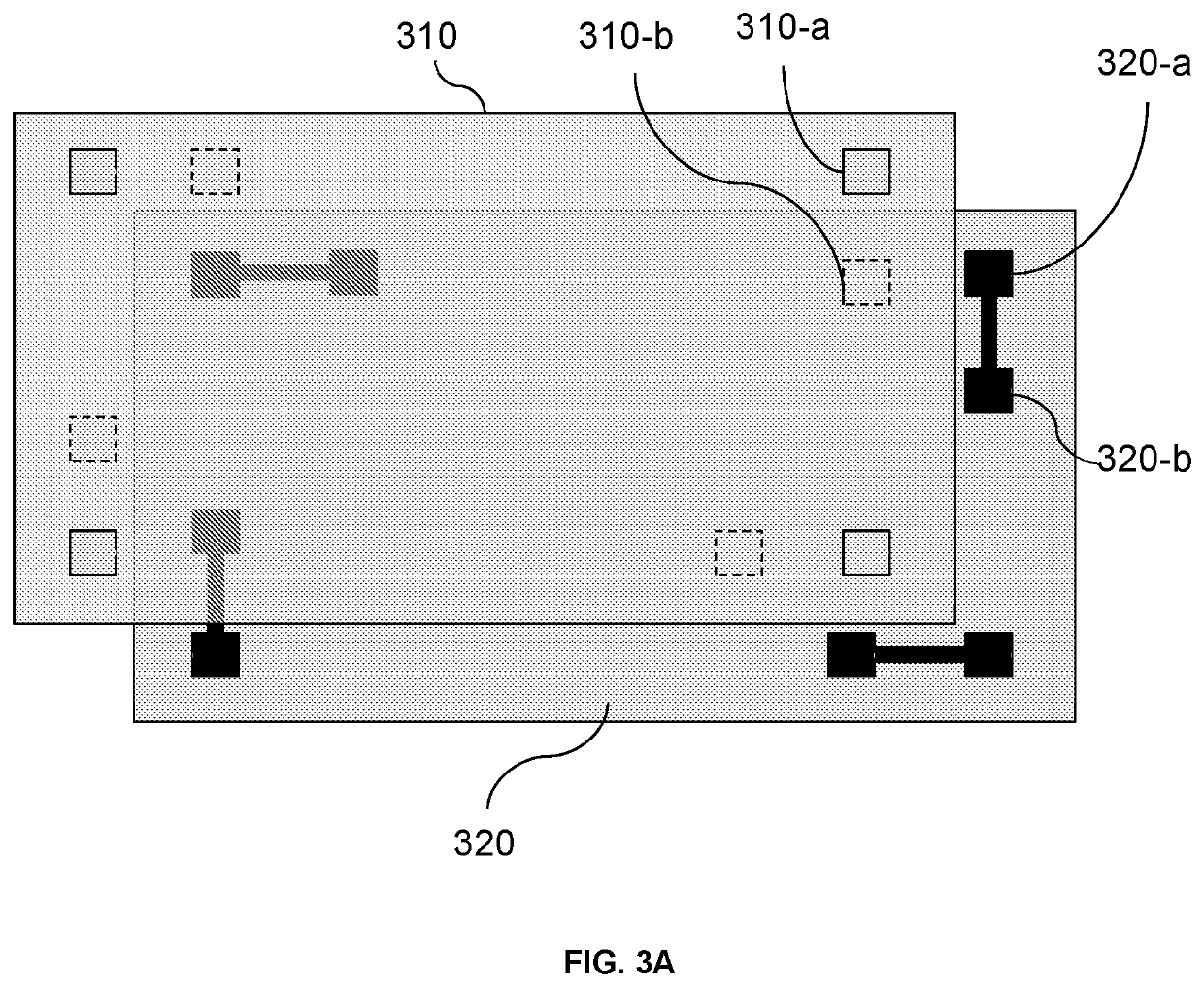
An alignment process for the transfer setup
a transfer setup and alignment technology, applied in the direction of semiconductor/solid-state device testing/measurement, semiconductor device details, semiconductor/solid-state device testing/measurement, etc., can solve the problem of complicated alignment over large-area substrates
- Summary
- Abstract
- Description
- Claims
- Application Information
AI Technical Summary
Benefits of technology
Problems solved by technology
Method used
Image

Examples
Embodiment Construction
[0028]While the present teachings are described in conjunction with various embodiments and examples, it is not intended that the present teachings be limited to such embodiments. On the contrary, the present teachings encompass various alternatives and equivalents, as will be appreciated by those of skill in the art.
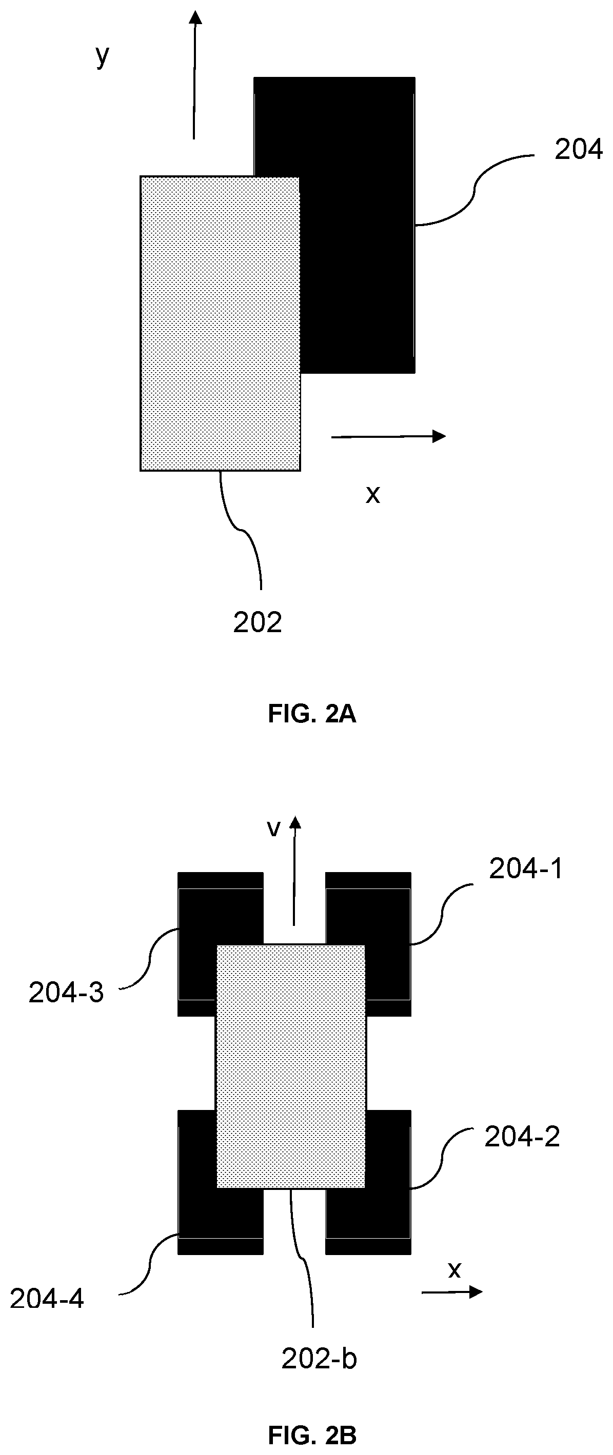
[0029]In LED display applications, where display pixels are single device LEDs, each LED is bonded to a driving circuit which controls the current flowing into the LED device. Here, the driving circuit may be a thin film transistor (TFT) backplane, a system substrate or a display wafer conventionally used in LCD or OLED display panels. Due to the typical pixel sizes (10-50 μm), bonding may be performed at a wafer-level scale. In this scheme, an LED wafer consists of isolated individual LED devices that are transferred and aligned, and bonded to a backplane or a display wafer which is compatible with an LED wafer pixel sizes and pitches. Various alignment techniques may ...
PUM
 Abstract
Description
Claims
Application Information