Capacitor

a technology of capacitors and capacitors, applied in the field of capacitors, can solve the problems of difficult manufacturing of ceramics and inability to conduct electricity, and achieve the effects of maximizing capacitance, maximizing capacity, and effectively reducing manufacturing costs

Active Publication Date: 2017-09-26
POINT ENG
View PDF3 Cites 0 Cited by
  • Summary
  • Abstract
  • Description
  • Claims
  • Application Information

AI Technical Summary

Benefits of technology

[0029]According to a capacitor of the present invention as described above, it has the following advantageous effects.
[0030]A capacitor of the present invention includes an electrode layer comprising a first electrode layer and a second electrode layer formed on the dielectric layer, wherein the first electrode layer and the second electrode layer are separated from each other, and at least a portion of the first electrode layer and at least a portion of the second electrode layer are disposed on the same surface, so that applying the electricity (i.e., electric current or electric voltage) becomes easy, and since the first and the second electrode layers function as the electrodes being charged with different polarity electrical charges respectively, manufacturing thereof becomes easy, and the structure thereof is simple.
[0031]The portion, which separates the first electrode layer and the second electrode layer, is disposed in the upper portion or the lower portion of the substrate, and the first electrode layer and the second electrode layer are formed so as to have different area from each other on the same surface, so that the capacitance can be maximized.
[0032]The substrate is comprised of a metallic material which can be anodized, and the dielectric layer is comprised of an anodized layer, and since the anodized layer formed by anodizing the substrate can be used as an upper and a lower dielectric layers without forming the upper and the lower dielectric layers separately, the manufacturing cost can be effectively reduced due to the simplified manufacturing process.
[0033]Furthermore, the dielectric layer comprises the upper and the lower dielectric layers formed on both of the upper and the lower surfaces of the substrate, and the electrode layer comprises the upper electrode layer formed on the upper surface of the upper dielectric layer and the lower electrode layer formed on the lower surface of the lowerer dielectric layer, and the upper electrode and the lower electrode layers are electrically connected so that the capacitance is maximized, and, at the same time, electricity can be applied to any one of the electrode layers without separately applying electricity to each of the electrode layers disposed on the upper and the lower side (of the dielectric layer), thus it is convenient.
[0034]A vertically penetrating through hole is formed at the substrate, and an internal dielectric layer continuously formed with (directly adjacent to) the upper dielectric layer and the lower dielectric layer is formed in the through hole, and a connecting electrode layer is located inside the internal dielectric layer so as to electrically connect the upper electrode layer and the lower electrode layer. Therefore, the upper electrode layer and the lower electrode layer can be effectively connected.

Problems solved by technology

A multi-layered ceramic capacitor can store electricity by stacking a plurality of ceramics layers and nickel layers using the principle that nickel conducts electricity since it is a metal, but ceramics cannot conduct electricity.
However, the capacitors of the prior art have complicated structures, therefore, there is a problem that manufacturing thereof is not that easy.

Method used


Image

  • Capacitor
  • Capacitor
  • Capacitor

Examples


exemplary embodiment 1

[Exemplary Embodiment 1]

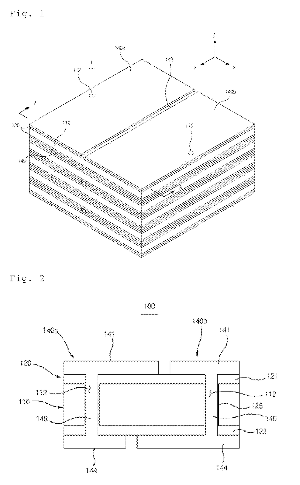
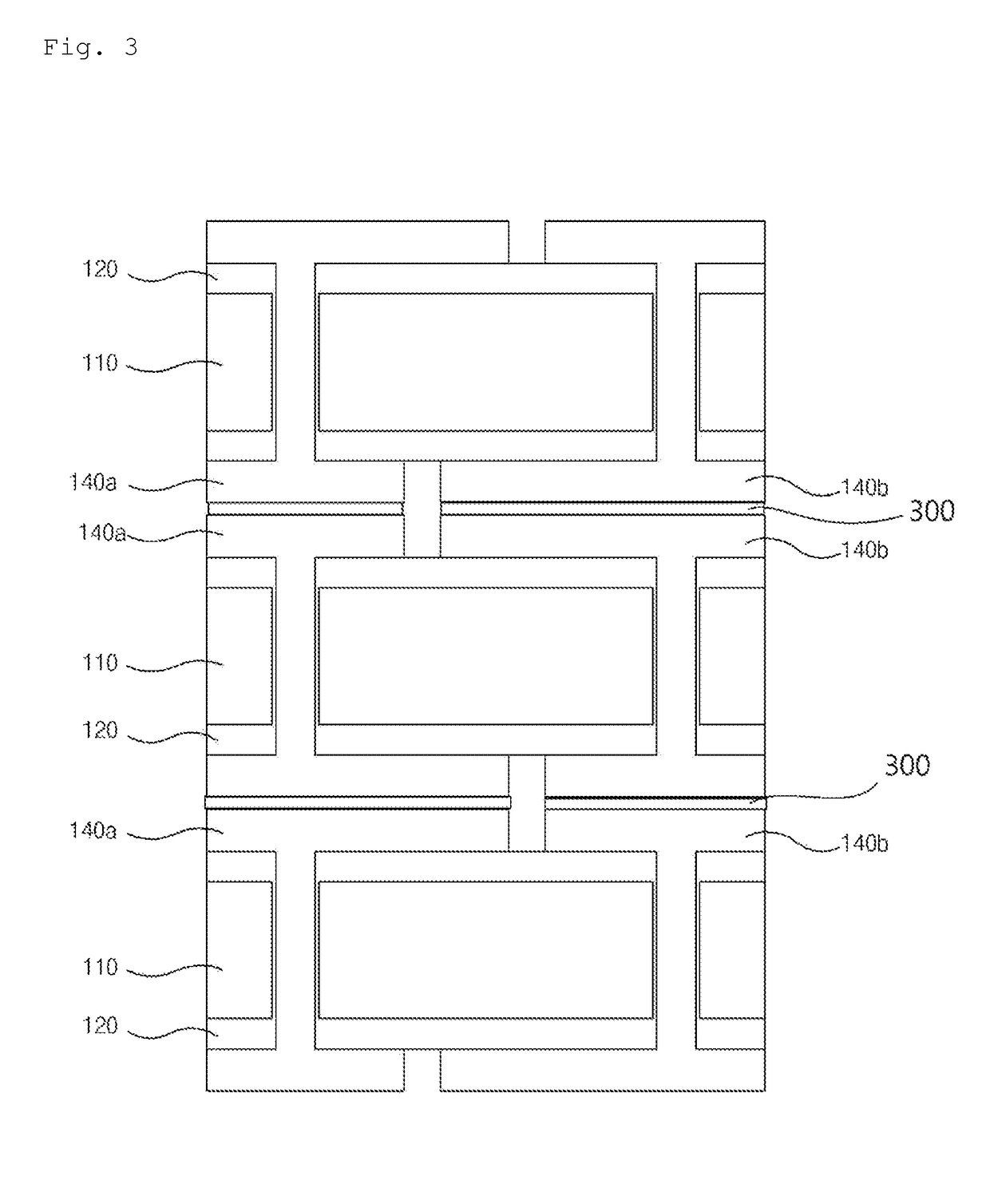
[0052]As illustrated in FIGS. 1 to 5, a capacitor 1 of the present exemplary embodiment includes a plurality of unit capacitors 100 sequentially stacked, each of the plurality of unit capacitors 100 including: a substrate 110; a dielectric layer 120 formed on the substrate 110; and an electrode layer comprising a first electrode layer 140a and a second electrode layer 140b formed on the dielectric layer 120, wherein the first electrode layer 140a and the second electrode layer 140b are separated from each other, the portion separating the first electrode layer 140a and the second electrode layer 140b is disposed on the upper side and the lower side of the substrate 110, and at least a portion of the first electrode layer 140a and at least a portion of the second electrode layer 140b are disposed on the same surface.

[0053]The substrate 110 is formed in the shape of a rectangular plate, and located in the center of the unit capacitor 100.

[0054]Although there is...

exemplary embodiment 2

[Exemplary Embodiment 2]

[0087]The description of the elements identical to those of the above Exemplary Embodiment 1 will be omitted.

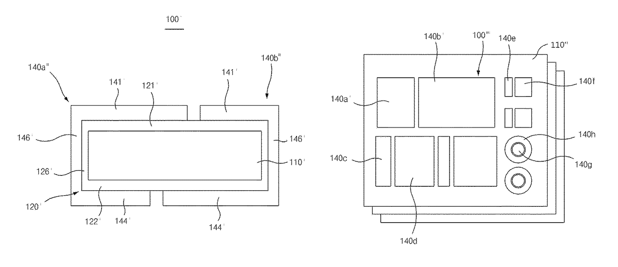
[0088]The unit capacitor 100′ of Exemplary Embodiment 2 has no hole in the substrate 110.

[0089]As illustrated in FIG. 6, the unit capacitor 100′ according to Exemplary Embodiment 2 includes: a side dielectric layer 126′ formed on the side surface of the substrate 110′ for connecting an upper dielectric layer 121′ and a lower dielectric layer 122′ along the side surface, wherein a side electrode layer 146′ is formed on the side dielectric layer 126′, and the upper electrode layer 141′ and the lower electrode layer 144′ are connected to the side electrode layer 146′.

[0090]The side dielectric layer 126′ is also an anodized layer formed by anodizing the substrate 110′ comprising aluminum.

[0091]The side dielectric layers 126′ are formed in the shape of a rectangle, and formed all over the right side surface and the left side surface of the substrate 110′ re...

exemplary embodiment 3

[Exemplary Embodiment 3]

[0094]The description of the elements identical to those of the above Exemplary Embodiments will be omitted.

[0095]As illustrated in FIG. 7, a capacitor according to Exemplary Embodiment 3 includes unit capacitors 100′″, wherein each of the unit capacitors 100′″ includes: a dielectric layer; and a plurality of electrode layers comprising the first electrode layers 140a′, 140c, 140e, and 140g, and the second electrode layers 140b′, 140d, 140f, and 140h, wherein the first electrode layers 140a′, 140c, 140e, and 140g, and the second electrode layers 140b′, 140d, 140f, and 140h, are separated from each other, and at least a portion of the first electrode layers 140a′, 140c, 140e, and 140g, and at least a portion of the second electrode layers 140b′, 140d, 140f, and 140h are disposed on the same surface, and a plurality of the unit capacitors 100′″ are formed on a large single substrate 110′″ to be separated from each other.

[0096]The plurality of unit capacitors 10...


PUM

PropertyMeasurementUnit
heightaaaaaaaaaa
dielectricaaaaaaaaaa
areasaaaaaaaaaa

Abstract

The present invention relates to a capacitor. The capacitor includes a substrate; a dielectric layer formed on the substrate; and an electrode layer comprising a first electrode layer and a second electrode layer formed on the dielectric layer, wherein the first electrode layer and the second electrode layer are separated from each other, and at least a portion of the first electrode layer and at least a portion of the second electrode layer are disposed on a same surface. With this configuration, applying the electricity becomes easy, and since the first and the second electrode layers function as the electrodes being charged with different polarity electrical charges respectively, manufacturing thereof becomes easy, and the structure thereof is simple.

Description

CROSS-REFERENCE TO RELATED PATENT APPLICATION[0001]This U.S. non-provisional patent application claims priority under 35 U.S.C. §119 of Korean Patent Application No. 10-2014-0115157 filed on Sep. 1, 2014 in the Korean Patent Office, the entire contents of which are hereby incorporated by reference.BACKGROUND[0002]1. Technical Field[0003]The present invention relates to a capacitor, more particularly, relates to a capacitor including an electrode layer comprising a first electrode layer and a second electrode layer formed on a dielectric layer, wherein the first electrode layer and the second electrode layer are separated from each other, and at least a portion of the first electrode layer and at least a portion of the second electrode layer are disposed on the same surface.[0004]2. Description of the Related Art[0005]Capacitor is used as a battery for storing or discharging electricity, or being utilized for its direct current blocking characteristics, and has a structure wherein a ...

Claims


Application Information

Patent Timeline
Patent Type & Authority Patents(United States)
IPC IPC(8): H01G4/30H01G4/38H01G4/005H01G4/012H01G4/12H01G4/228
CPCH01G4/30H01G4/005H01G4/012H01G4/12H01G4/38H01G4/228
Inventor AHN, BUM MOPARK, SEUNG HOSONG, TAE HWAN
Owner POINT ENG
Why Eureka
Try Eureka