Semiconductor device

a technology of semiconductors and devices, applied in the field of semiconductor devices, can solve the problems of difficult in terms of computation time to acquire the solution by the neumann type computer, and difficult to extract parallelism from a program

Active Publication Date: 2016-03-03
HITACHI LTD
View PDF0 Cites 22 Cited by
  • Summary
  • Abstract
  • Description
  • Claims
  • Application Information

AI Technical Summary

Benefits of technology

[0018]A problem, configuration and effect except the abovementioned those will be clarified by the description of the following embodiment.

Problems solved by technology

However, it is not easy to extract parallelism from a program in which serial algorithm is written in the form of instruction strings.
It is known that search by topology for a ground state of the Ising model to be a nonplanar graph is an NP-hard problem.
As the search of the ground state of the Ising model is the NP-hard problem as described above, it is difficult in terms of computation time to acquire the solution by the Neumann type computer.
In addition, it can also be imagined that bias exists individually in each person.
That is, to realize the more number of spins, a large number of lasers are required to be arranged and a superconducting device that requires advanced cooling technique has a limit.

Method used


Image

  • Semiconductor device
  • Semiconductor device
  • Semiconductor device

Examples


Embodiment Construction

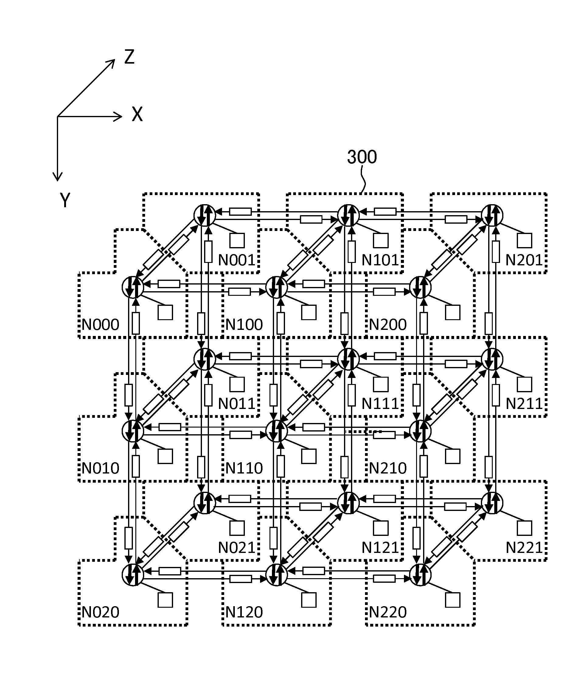
[0050]Ising model can be given for an example of a representative interaction model in the world of physics. The Ising model is based upon spin that takes two states of +1 and −1 (or upper and lower) and is defined by an interaction coefficient that determines interaction between two spins and an external magnetic field coefficient which is bias to individual spin. This embodiment will be described using Ising chip which is a device that can manage the Ising model for an example for means for making the computation of the interaction model. However, the present invention provides technique for computing a value of a variable in a function at high speed when a value of the function expressing a general interaction model is converged on a desired value and application is not limited to the Ising model. Besides, although the device in the embodiment is called the Ising chip for convenience, the device in the embodiment may also be applied to a model except the Ising model.

[0051]One exa...


PUM


Abstract

An object of the present invention is to realize an example of configuration that approximately represents a state of quantum spin in a semiconductor device where components as a basic configuration unit are arrayed so as to search a ground state of Ising model. There is disclosed a semiconductor device provided with plural units each of which is equipped with a first memory cell that stores a value which represents one spin of the Ising model by three or more states, a second memory cell that stores an interaction coefficient showing interaction from another spin which exerts interaction on the one spin and a logical circuit that determines the next state of the one spin on the basis of a function having a value which represents a state of the other spin and the interaction coefficient as a constant or a variable.

Description

CLAIM OF PRIORITY[0001]The present application claims priority from Japanese application serial no. JP2014-176127, filed on Aug. 29, 2014, the content of which is hereby incorporated by reference into this application.FIELD OF THE INVENTION[0002]The present invention relates to a device that makes computation for an interaction model.BACKGROUND OF THE INVENTION[0003]Currently, a mainstream of computer architecture lies in Neumann type computer. The basic operation of the Neumann type architecture is to sequentially execute instruction strings. Enhancement in the performance of a computer has mainly depended upon the enhancement of a clock frequency. However, recently, in place of the clock frequency that reaches the peak, a method of realizing the enhancement of performance with parallel processing by multicoring is a mainstream.[0004]In the parallel processing by multicoring, performance is enhanced by finding a location where parallel execution is possible in serial instruction st...

Claims


Application Information

Patent Timeline
Patent Type & Authority Applications(United States)
IPC IPC(8): H03K19/00
CPCH03K19/0002G11C11/1659G11C11/5607G06N20/00G06N7/01
Inventor YOSHIMURA, CHIHIROYAMAOKA, MASANAOHAYASHI, MASATO
Owner HITACHI LTD
Why Eureka
Try Eureka