Semiconductor device and information processing system

a technology of information processing system and semiconductor device, which is applied in the field of semiconductor device, can solve the problems of substantially impossible to search for all ground states in searching for ground states, and achieve the effect of facilitating the extension of the device's scale and reducing the cos

Active Publication Date: 2018-04-17
HITACHI LTD
View PDF8 Cites 1 Cited by
  • Summary
  • Abstract
  • Description
  • Claims
  • Application Information

AI Technical Summary

Benefits of technology

[0017]According to the present invention, as the semiconductor device that searches for a ground state of the Ising model can supply randomness by a few random number generators, the cost reduction and the extension in scale of the device are facilitated.

Problems solved by technology

It is known that the acquisition of a ground state of the Ising model which is a non-planar graph by topology is an NP-hard problem.
Since there are a large number of the combinations of possible states of spins included in the Ising model, it is substantially impossible to search for all ground states in searching for a ground state.
However, since an evil effect also occurs that local optimum solution is selected by narrowing down and only an approximate ground state is acquired, a method of enabling acquiring better solution by avoiding local solution found in a process of a search is required.

Method used


Image

  • Semiconductor device and information processing system
  • Semiconductor device and information processing system
  • Semiconductor device and information processing system

Examples


first embodiment

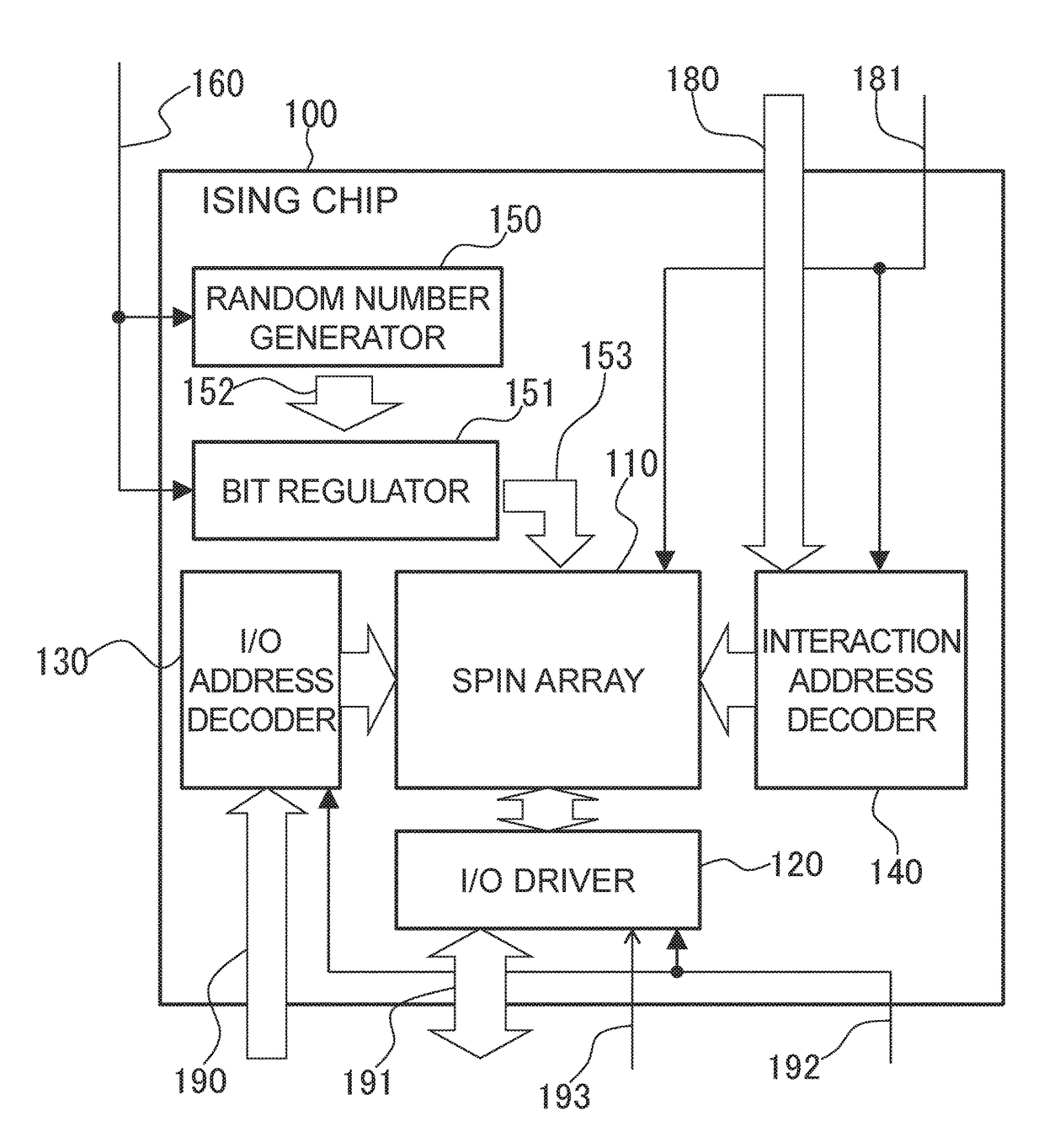
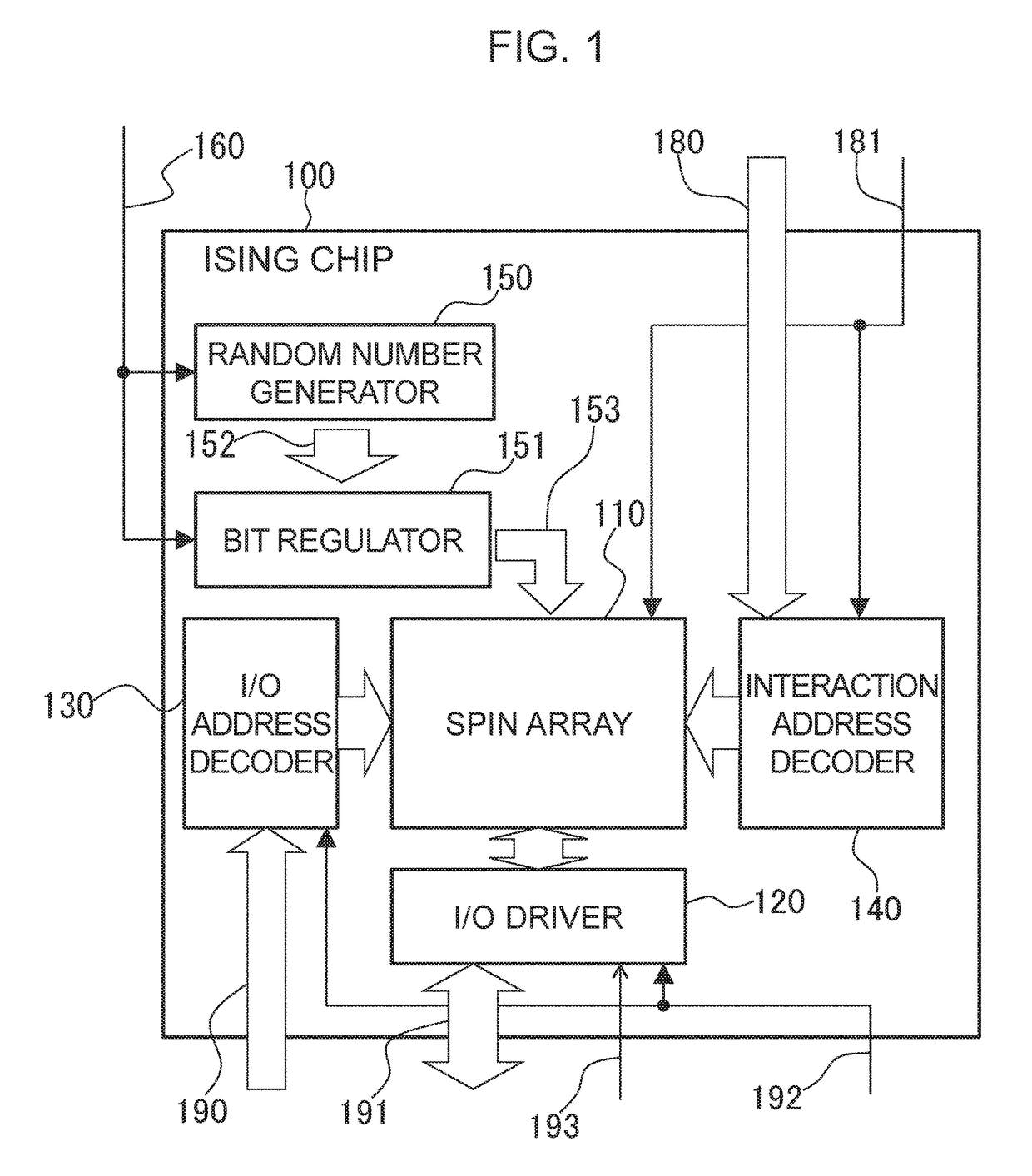
[0036]An Ising model is a statistical-mechanical model used in explaining behavior of a ferromagnetic substance. The Ising model is defined by plural spins that take a binary state of +1 or −1, an interaction coefficient representing the intensity of interaction between spins, and an external magnetic field coefficient representing the intensity of an external magnetic field that acts on each spin.

[0037]In the Ising model, energy at that time can be calculated on the basis of a spin array, interaction coefficients and external magnetic field coefficients respectively provided.

[0038]An energy function E(σ) of the Ising model is defined by the following mathematical expression 1. In the mathematical expression 1, σi and σj are values of i“th” and j“th” spins, Ji,j is an interaction coefficient between the i“th” and j“th” spins, Ji,j is a coefficient of an external magnetic field that acts on the i“th” spin, is combination of adjacent all spins (i and j), and σ represents an array of ...

second embodiment

[0102]As described in the first embodiment, random bits are asynchronously propagated in each spin unit 300. Generally, since delay due to the buffer 821 is small, a situation that the same random bit is input to adjacent spin units 300 in the spin array 110 may occur. Especially, when the random number generation clock 160 of the random number generator 150 is slow, this trend becomes remarkable and the same random bit is input to multiple spin units 300. In such a situation, since behavior of an inverting logical circuit is uniform in adjacent spin units, there is possibility that capability to escape from local solution is deteriorated.

[0103]In a second embodiment, a configuration that reduces the abovementioned problems and can supply higher randomness to each spin unit will be described. In comparison with the first embodiment, since there is difference between the propagation path of random bits shown in FIG. 6 and the inside of the spin unit 300 shown in FIG. 9, the differenc...

third embodiment

[0107]As described in the first embodiment, since random bits are asynchronously propagated in each spin unit, delay when they are propagated in one spin unit is small. However, when a spin array includes extremely multiple spin units, time until a random bit input from a bit regulator reaches a spin unit at a termination is also extended. In the meantime, in a process in which a ground state of an Ising model is searched, bit probability is required to be lowered as time elapses. At this time, at timing for switching bit probability, such unevenness of bit probability that bit probability of a spin unit close to a bit regulator is low and bit probability of a spin unit far from the bit regulator remains high occurs. Such the unevenness of bit probability may have a bad effect on precision of the search for a ground state.

[0108]In a third embodiment, a configuration that reduces the abovementioned problems and inhibits the unevenness of bit probability even if multiple spin units ar...


PUM


Abstract

A spin unit provided with a memory cell that stores a value of one spin of an Ising model, a memory cell that stores an interaction coefficient from an adjacent spin which interacts with the corresponding spin, a memory cell that stores an external magnetic field coefficient of the one spin and circuits that determine the next state of the one spin on the basis of a product of a value of each adjacent spin and the corresponding interaction coefficient and the external magnetic field coefficient is configured, the semiconductor device is provided with a spin array where the plural spin units are arranged and connected on a two-dimensional plane on a semiconductor substrate, a random number generator and a bit regulator, the bit regulator operates output of the random number generator and supplies a random bit to all spin units in the spin array via one wire.

Description

TECHNICAL FIELD[0001]The present invention relates to a semiconductor device that searches for a ground state of an Ising model, and especially relates to a semiconductor device that simulates spin of the Ising model as a flip-flop of a CMOS device.BACKGROUND ART[0002]The Ising model is a statistical-mechanical model for explaining behavior of a magnetic substance. The Ising model is defined by spin that takes a binary of +1 and −1 (or 0 and 1 or upward and downward), an interaction coefficient showing interaction between spins and an external magnetic field coefficient for every spin. The Ising model enables calculating energy at that time on the basis of a provided spin array, interaction coefficients and an external magnetic field coefficient.[0003]A search for a ground state of the Ising model is equivalent to an optimization problem for acquiring an array of spins that minimizes an energy function of the Ising model. It is known that the acquisition of a ground state of the Isi...

Claims


Application Information

Patent Timeline
Patent Type & Authority Patents(United States)
IPC IPC(8): G06F17/18G06F7/58G11C11/16G06N99/00G06N7/00H03L7/26H01L27/11
CPCG06F7/588G06F17/18G06N7/005H01L27/11H03L7/26G11C11/16G06N99/002G06N10/00G06N7/01H10B10/00
Inventor HAYASHI, MASATOYAMAOKA, MASANAOYOSHIMURA, CHIHIRO
Owner HITACHI LTD
Why Eureka
Try Eureka