Display device and driving method thereof

a technology of a display device and a driving method, which is applied in the direction of electric digital data processing, instruments, computing, etc., can solve the problem of not sufficiently and achieve the effect of preventing or suppressing the flash phenomenon

Active Publication Date: 2016-03-24
JAPAN DISPLAY INC
View PDF2 Cites 6 Cited by
  • Summary
  • Abstract
  • Description
  • Claims
  • Application Information

AI Technical Summary

Benefits of technology

[0010]An object of the present invention is to provide a display device and a driving method thereof which are able to prevent or suppress a flash phenomenon at the time of power source ON of the display device.

Problems solved by technology

However, according to the operation described above, the potential of each of the terminals of the driving TFT 6 becomes inconstant at the time of the main power source ON, and an unconsidered potential difference may be generated due to coupling between the power source line 18 and an internal node, and thus the flash phenomenon is not sufficiently suppressed.

Method used


Image

  • Display device and driving method thereof
  • Display device and driving method thereof
  • Display device and driving method thereof

Examples


Embodiment Construction

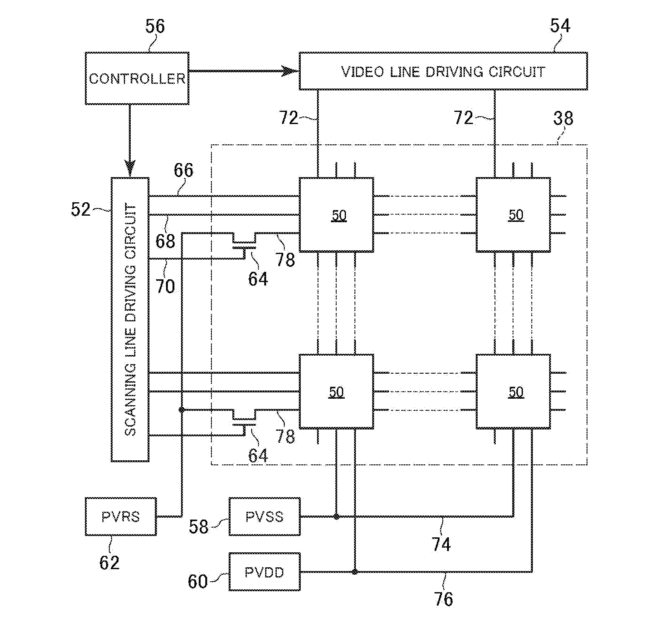
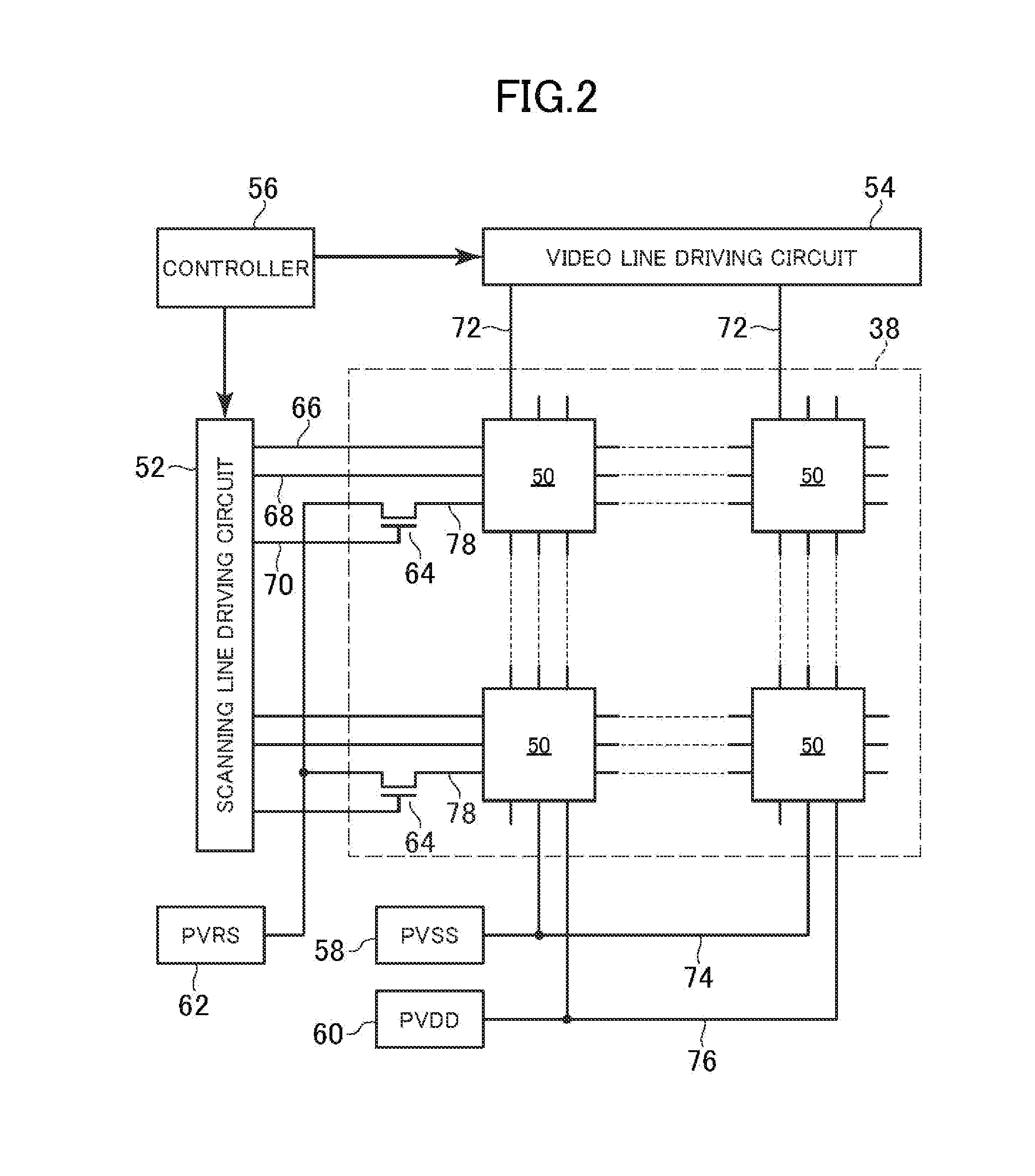
[0023]Hereinafter, an image display device which is an embodiment of the present invention (hereinafter, referred to as an embodiment) will be described with reference to the drawings. The image display device is an active matrix type organic EL display device in which OLEDs are provided as light emitting elements.

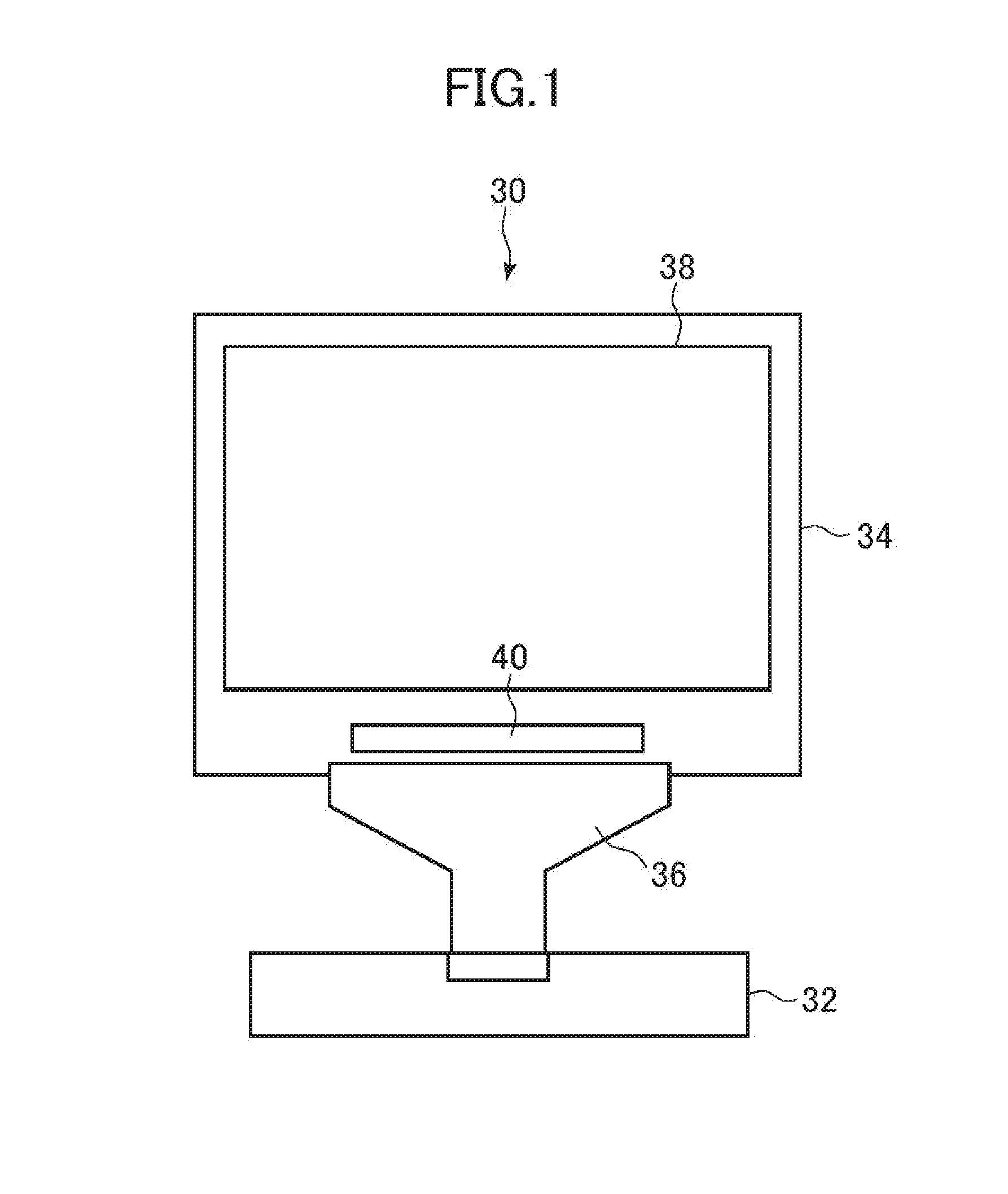
[0024]FIG. 1 is a schematic diagram illustrating a schematic configuration of an organic EL display device 30 according to the embodiment. The organic EL display device 30 includes a main body circuit 32, a display substrate 34, and a connection substrate 36. A display unit 38 in which OLEDs and pixel circuits corresponding to pixels of a display image are arranged is formed on the display substrate 34. As a control unit controlling the operation of the display unit 38, a driving circuit supplying various signals to the pixel circuit, and a controller generating a timing signal or the like which is supplied to the driving circuit are disposed. The control unit is arranged ...


PUM


Abstract

A flash phenomenon of OLEDs at the time of power source ON of a display device is suppressed. The OLED emits light when reference potentials VSS and VDD are applied from power source lines to the OLED's cathode and anode respectively. While the anode can be connected to one of the power source line via a driving TFT and a lighting switch, a reset potential VRS can be applied to the anode via a reset switch and the driving TFT. The lighting switch is turned OFF and the reset switch and the driving TFT are turned ON so that VRS is applied to the anode, before starting the application of the reference potentials to the power source lines. Following this state, the application of the reference potentials to the power source lines starts, and thus a normal operation of allowing the OLED to emit light starts.

Description

CROSS-REFERENCE TO RELATED APPLICATION[0001]The present application claims priority from Japanese application JP2014-189782 filed on Sep. 18, 2014, the content of which is hereby incorporated by reference into this application.BACKGROUND OF THE INVENTION[0002]1. Field of the Invention[0003]The present invention relates to a display device and a driving method thereof using a self-light emitting element which emits light by voltage application.[0004]2. Description of the Related Art[0005]As an electro-optic element used in a self-light emitting display device, an organic electroluminescence (EL) element has been known. The organic electroluminescence element is generally referred to as an organic light emitting diode (OLED), and is one type of light emitting diode.[0006]FIG. 9 is a schematic circuit diagram of a pixel circuit 2 which is arranged in a display unit of an organic EL display panel. Each pixel circuit 2 includes an OLED 4 which is a light emitting element, a thin film tra...

Claims


Application Information

Patent Timeline
Patent Type & Authority Applications(United States)
IPC IPC(8): G09G3/32
CPCG09G2300/0426G09G3/3258G09G3/3233G09G2300/0861G09G2310/0245G09G2330/021G09G2330/025G09G2330/026
Inventor MORITA, TETSUOKIMURA, HIROYUKISHIBUSAWA, MAKOTONAKAYAMA, HIROSHITABATAKE, HIROSHIUMEDA, YUTAKA
Owner JAPAN DISPLAY INC
Why Eureka
Try Eureka