Display device and method for fabricating the same

a technology of a display device and a manufacturing method, which is applied in the direction of electrical apparatus construction details, printed circuit non-printed electric components association, instruments, etc., can solve the problems of damage to line patterns and data driving ic of the carrier, and the carrier may include a relatively weak material. torn by stress, the effect of reducing or preventing the stress induced on the carrier

Active Publication Date: 2016-03-31
SAMSUNG DISPLAY CO LTD
View PDF6 Cites 4 Cited by
  • Summary
  • Abstract
  • Description
  • Claims
  • Application Information

AI Technical Summary

Benefits of technology

[0009]Exemplary embodiments of the present invention are directed to a display device configured to reduce or prevent damage to line patterns (e.g., conductive line patterns) and a driving IC of carriers, and to a method of manufacturing the display device.
[0028]A carrier according to exemplary embodiments of the present invention includes a plurality of first and second connectors spaced apart from each other. Accordingly, the first and second connectors may extend in a direction of tensile force caused when a source PCB and a display panel are bent. Thus, the stress induced on the carrier may be reduced or prevented, and damage on line patterns and data driving IC of the carrier may be reduced or prevented.

Problems solved by technology

For example, tape carriers including a relatively weak material may be torn by the stress.
This may cause damage on line patterns and driving integrated circuit (IC) of the tape carriers.

Method used


Image

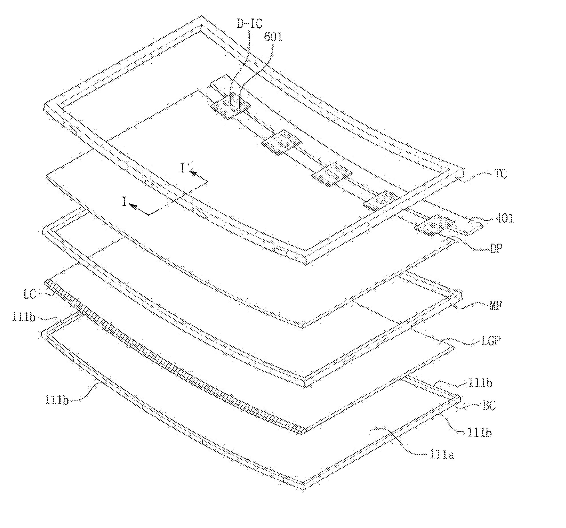
  • Display device and method for fabricating the same
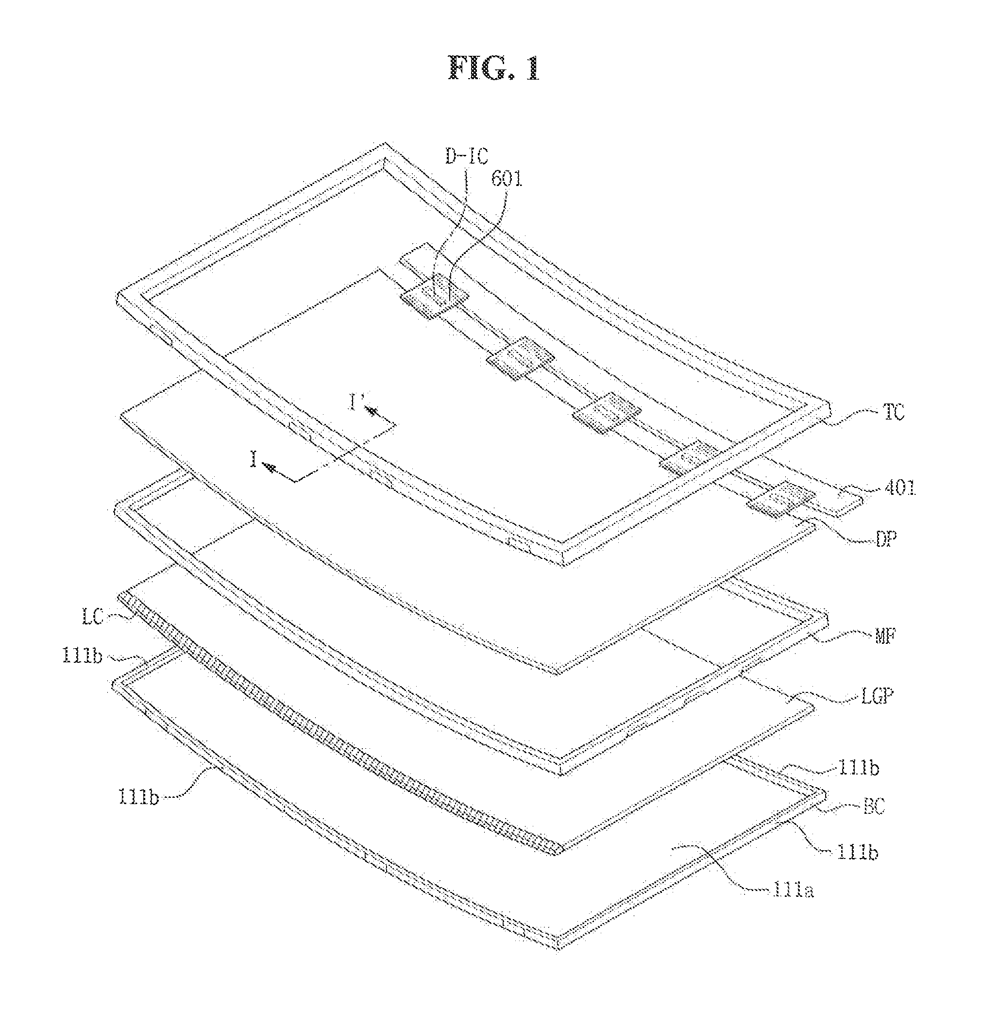
  • Display device and method for fabricating the same
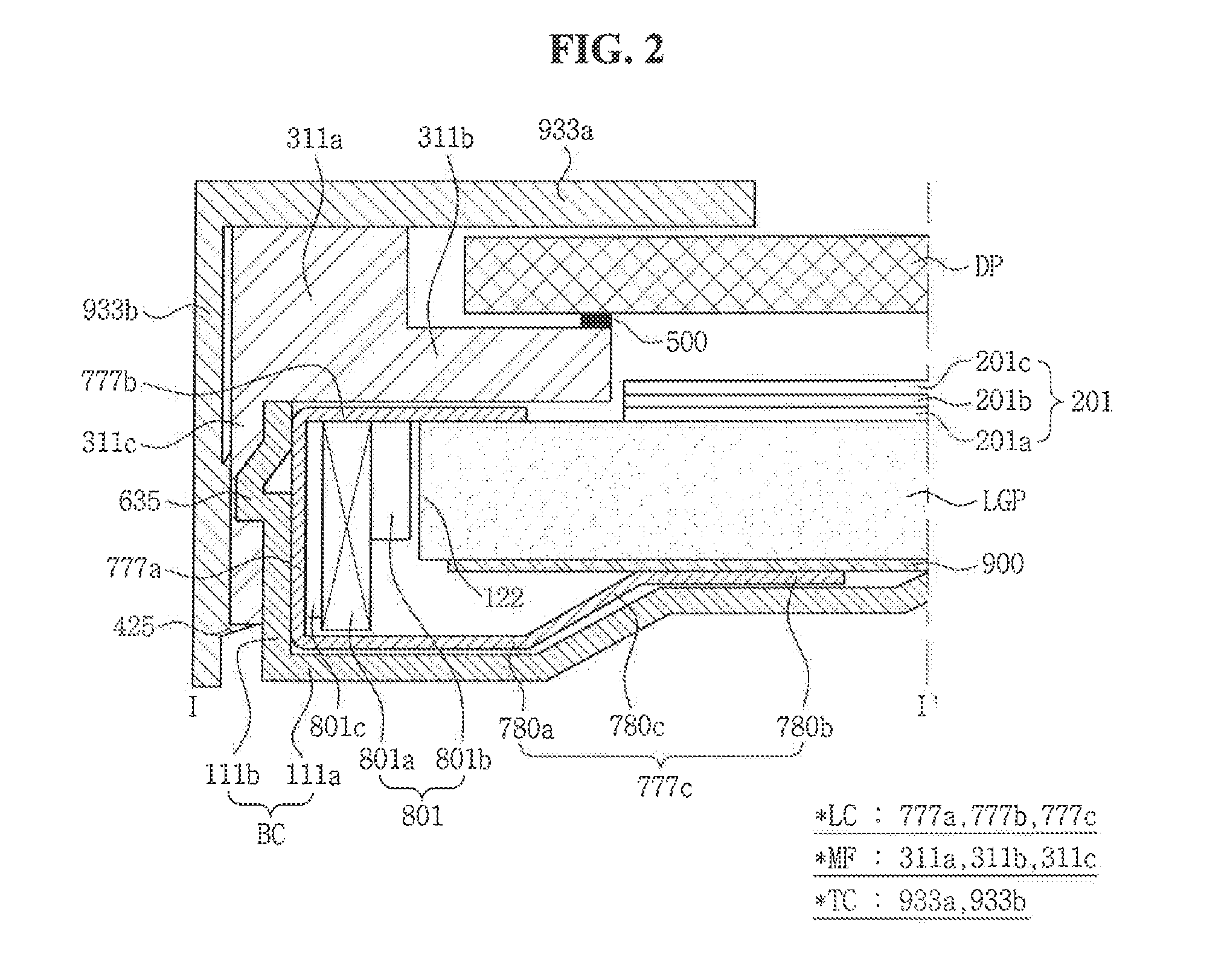
  • Display device and method for fabricating the same

Examples


Embodiment Construction

[0039]Hereinafter, exemplary embodiments of the present invention will be described in more detail with reference to the accompanying drawings. The present invention may, however, be embodied in many different forms and should not be construed as being limited to the embodiments set forth herein. Like reference numerals may refer to like elements throughout the specification and drawings.

[0040]In the drawings, thicknesses may be illustrated in an enlarged manner in order to clearly describe a plurality of layers and areas. Like reference numbers may be used to denote like elements throughout the specification and drawings. When an element or layer is referred to as being “on”, “engaged to”, “connected to” or “coupled to” another element or layer, it may be directly on, engaged, connected or coupled to the other element or layer, or intervening elements or layers may be present.

[0041]The spatially relative terms “below”, “beneath.”, “lower”, “above”, “upper”, and the like, may be use...


PUM

PropertyMeasurementUnit
areaaaaaaaaaaa
shapesaaaaaaaaaa
shapeaaaaaaaaaa

Abstract

A display panel includes a display panel having a curved shape and a printed circuit hoard (PCB). At least one carrier connects the display panel and the PCB. At least one driving integrated circuit (driving IC) is disposed on each carrier. Each carrier includes a body and at least one connector extending from the body. Each connector is spaced apart from each other connector.

Description

CROSS-REFERENCE TO RELATED APPLICATION[0001]This application claims priority under 35 U.S.C. §119 to Korean Patent Application No. 10-2014-0130140, filed on Sep. 29, 2014, in the Korean intellectual Property Office, the disclosure of which is incorporated by reference herein in its entirety.1. TECHNICAL FIELD[0002]Exemplary embodiments of the present invention relate to a display device, and more particularly to a method of manufacturing the display device.2. DISCUSSION OF RELATED ART[0003]A liquid crystal display (LCD) is a type of flat panel display (FPD). LCDs may include two substrates with electric field generating electrodes (e.g., pixel electrodes and common electrodes) disposed thereon and a liquid crystal layer disposed therebetween. Upon applying voltage to the electrodes, liquid crystal molecules of the liquid crystal layer are rearranged, thereby adjusting an amount of light that is transmitted.[0004]As LCD devices are used as a display device of television receivers, a ...

Claims


Application Information

Patent Timeline
Patent Type & Authority Applications(United States)
IPC IPC(8): G02F1/1345H05K7/02
CPCH05K7/02G02F1/13452G02F1/133305
Inventor CHO, JOOWOANNA, JEONGKYUNLEE, SEUNGHWANCHEONG, BYOUNGHO
Owner SAMSUNG DISPLAY CO LTD
Why Eureka
Try Eureka